Version: 13. September 2004
7
proach. Unpleasant overloading effects from insufficient regulating voltages
at low speech frequencies is thus minimized. The decay is regulated by R72.
R76-R77 defines the attack. You can attach an optional 100 µA instrument
at P5 to give a relative field strength indication. The combined IF/AF
regulation is more than 90 dB!!! Input signals of S9+60dB are regulated
distorsion free. After a further 2800 Hz low pass at R78-C110, the signal is
fed to an 800 mW AF PA in IC11. T16 blocks the regulating voltage during
transmission. T17 blocks the AF amplifier during T/R switching to reduce
switching noise.
6. Side band oscillator:
The carrier needed for modulation and demodulation is generated by the
capacitative three point circuit (Colpitts) at T20. The produced frequency is
determined by the parallel coupled 8 MHz crystals Q6-Q7. The tuning diodes
D29-D30 in conjunction with L7 leaves a tuning range of some 6 kHz for
the VXO. P7 adjust the RF signal to some 300 mVpp and leads the signal via
C97-C137 to the product detector of IC9 and the balanced modulator of
IC16. The tuning voltage for D29-D30 comes from potentiometers P8 and
P11, switched by the analog switch in IC12. This circuit gives the necessary
carrier frequencies for the different modulation types, and for the varying
center frequencies, in an easy way.
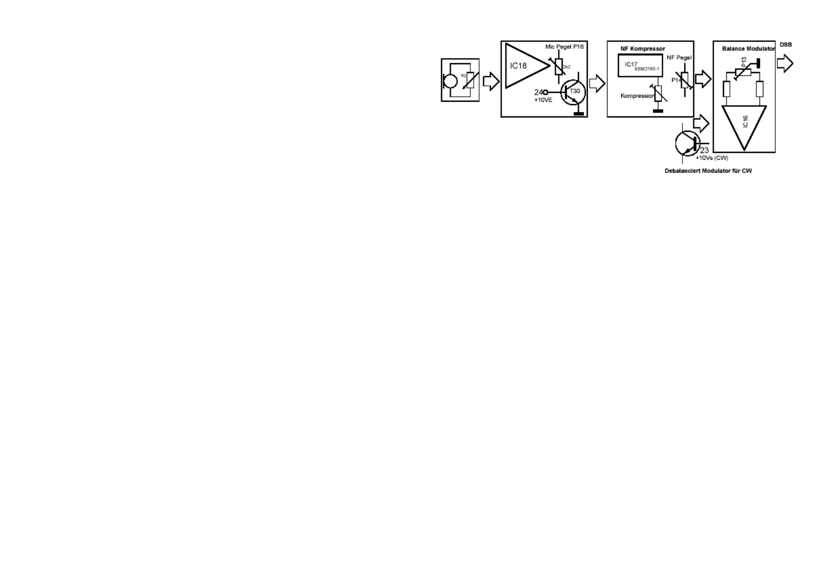
7. 8MHz SSB generation:
The microphone signal is led via the mic gain potentiometer to the input of
the preamplifier IC18. The circuit of C150-Dr12-C149 reduces transmitter RF
in the modulation amplifier. The amplification of the stage is set to some
26 dB byt R126-R127. C148-C147 cuts speech frequencies below 300 Hz.
The level of the amplified microphone signal is adjusted in P16 before
going into the dynamic compresson IC17. The utilized IC SSM3165 from
Analog Devices was made for studio techniques and gives a compression of
max. 15:1, that is 15 dB input dynamic range for 1 dB og output dynamic
range. The [klirrfaktor - please change!!!] of the output signal is less than 1
%. This compressor will allow the PA to swing to the QRP allowance of 10W
PEP. This gives a subjective power level of some 50W uncompressed!! P15
allows individual adjustment of the compression. P14 leads the compressed
signal on to the balanced modulator of IC15. C139 gives a further low pass
cut off. The modulator uses the universal Gilbert cell NE612. The internal
oscillator isn’t used. C137 leads the appropriate signal in from T20. P13
adjust the carrier suppression. In CW mode the modulator is debalanced by
T29-R116, that is the carrier signal is no longer suppressed, but led on to
the modulator output. to avoid swing in problems at the modulator at T/R
switching, IC16 is at permanent power. For this reason T30 blocks the
modulation path during reception and disallows a DSB signal at open micro-
phone. This guarantees against feed through to the high amplification IF.
The 8 MHz DSB signal is led from pin 5 of IC15 to T14. The collector of T14
sees the transformed filter terminating resistance via the 1:1 transformer of
Tr8. This gives a stage amplification of 6 dB in conjunction with R66.
During reception T15 breaks the emitter circuit of T14, blocking the collec-
tor-basis voltage at R65. Pin 12 on the pc board is at ground potential at
this moment, also blocking the PIN diode D22. This serves to dampen the
residual carrier signal at the input of IC9. During transmission the amplified
8 MHz DSB signal is led the other way through the Cohn filer and shows up
a an SSB signal with suppressed carrier at Tr7. The MOSFET T23 gives a
voltage amplification of some 6 dB. Choice of side band is by the carrier
frequency from T20. C85 couples the SSB signal to the amplifier at T23. A
positive voltage at the source of T23 is used to adjust TX power. In CW
mode, keying is done by breaking the drain voltage at pin 30. Tr6 trans-
forms the output impedance determined by R98 to the 50 Ohm level. PIN
diode D14 leads the 8 MHz signal to the IF port of M1. D13 blocks and T12-
T13 are decoupled.