EasyManuals Logo

Quectel BG95 User Manual

Quectel BG95
48 pages
To Next Page IconTo Next Page
To Previous Page IconTo Previous Page
Page #25 background imageLoading...
Page #25 background image
LPWA Module Series
BG95&BG96 Compatible Design
BG95&BG96_Compatible_Design 24 / 47
4.2. Turn-on
The turn-on method of BG95 is the same as that of BG96. BG95 can be powered on through pressing
PWRKEY for 500ms to 1000ms, and BG96 can be powered on through pressing PWRKEY for at least
500ms.
The PWRKEY pin of BG95/BG96 is internally pulled up to an internal voltage in the Qualcomm chipset,
and its output voltage is the internal voltage minus a diode drop in the chipset. For BG95, the expected
output voltage of PWRKEY is 1.5V. For BG96, the expected output voltage of PWRKEY is 0.8V.
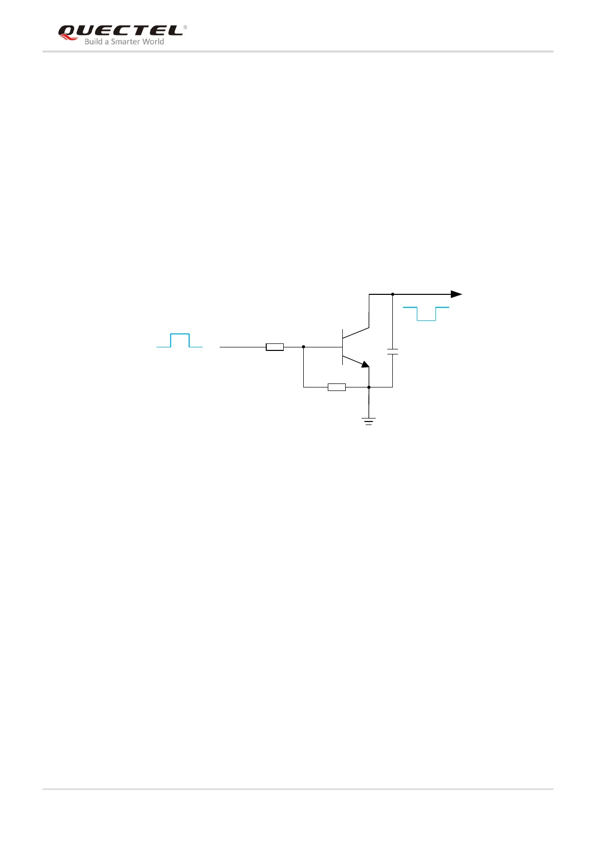
The following is a reference design for the turn-on circuit of BG95 and BG96.
PWRKEY
4.7K
47K
T2
10nF
Turn-on pulse
Figure 4: PWRKEY Driving Circuit for Module Turn-on (BG95/BG96)
The power-on scenario of BG95 and BG96 is illustrated in the figure below.

Questions and Answers:

Question and Answer IconNeed help?

Do you have a question about the Quectel BG95 and is the answer not in the manual?

Quectel BG95 Specifications

General IconGeneral
ChipsetQualcomm MDM9205
LTE CategoryCat M1/Cat NB2
GNSSGPS/GLONASS/BeiDou/Galileo/QZSS
Operating Temperature-40°C to +85°C
Storage Temperature-45°C to +90°C
SIM Interface1.8V/3V
Dimensions23.6 mm × 19.9 mm × 2.2 mm
LTE Cat NB2 Data Rate127kbps (DL), 158kbps (UL)
EGPRS Data Rate296kbps (DL), 236.8kbps (UL)
Supply Voltage Range3.3V to 4.3V
Power ConsumptionPSM: 3.2 μA
InterfacesUART, USB 2.0, I2C, SPI, GPIO, ADC
SMSText and PDU Mode
ProtocolsTCP/UDP/PPP
CertificationsFCC, IC, CE, RCM, PTCRB, GCF
Frequency BandsGSM: 850/900/1800/1900MHz

Related product manuals