LTE-A Module Series
EG06 Hardware Design
EG06_Hardware_Design 50 / 89
PCM_CLK
PCM_SYNC
PCM_OUT
MSB
LSB
PCM_IN
125us
MSB
1 2 3231
LSB
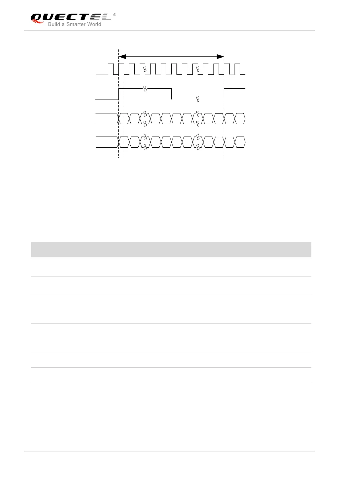
Figure 24: Auxiliary Mode Timing
The following table shows the pin definition of PCM and I2C interfaces which can be applied on audio
codec design.
Table 15: Pin Definition of PCM and I2C Interfaces
Clock and mode can be configured by AT command, and the default configuration is master mode using
short frame synchronization format with 2048kHz PCM_CLK and 8kHz PCM_SYNC. Please refer to
document [1] for details about AT+QDAI command.
1.8V power domain.
If unused, keep it open.
1.8V power domain.
If unused, keep it open.
PCM data frame
synchronization
signal
1.8V power domain. In master mode, it
is an output signal. In slave mode, it is
an input signal.
If unused, keep it open.
1.8V power domain. In master mode, it
is an output signal. In slave mode, it is
an input signal.
If unused, keep it open.
Require an external pull-up to 1.8V
Require an external pull-up to 1.8V

 Loading...