LPWA Module Series
BG950A-GL&BG951A-GL_Hardware_Design
32
/89
Figure 4: Power Supply Limits During Burst Transmission
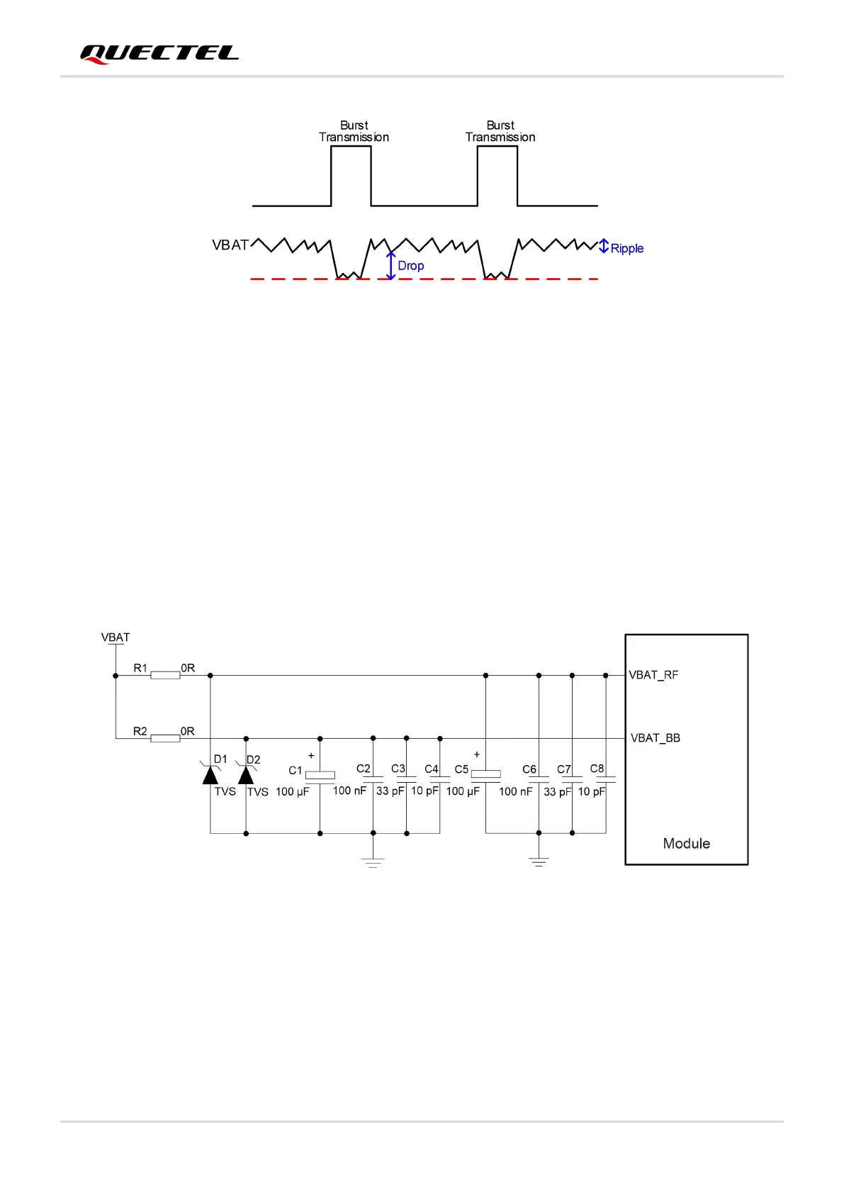
To decrease voltage ‘s drop, a bypass capacitor of about 100 μF with low ESR should be used, and a
multi-layer ceramic chip (MLCC) capacitor array should also be reserved due to its ultra-low ESR. It is
recommended to use three ceramic capacitors for composing the MLCC array (100 nF, 33 pF, 10 pF),
and place these capacitors close to VBAT pins. The main power supply from an external application must
be a single voltage source and can be expanded to two sub paths with the star structure. The width of
VBAT_BB trace should be no less than 1 mm. The width of VBAT_RF trace should be no less than 1 mm.
In principle, the longer the VBAT trace is, the wider it will be.
In addition, to ensure the stability of the power supply, it is necessary to add two high-power TVSs at the
front end of each power supply. Reference circuit of power supply is shown as below:
Figure 5: Star Structure of the Power Supply

 Loading...


