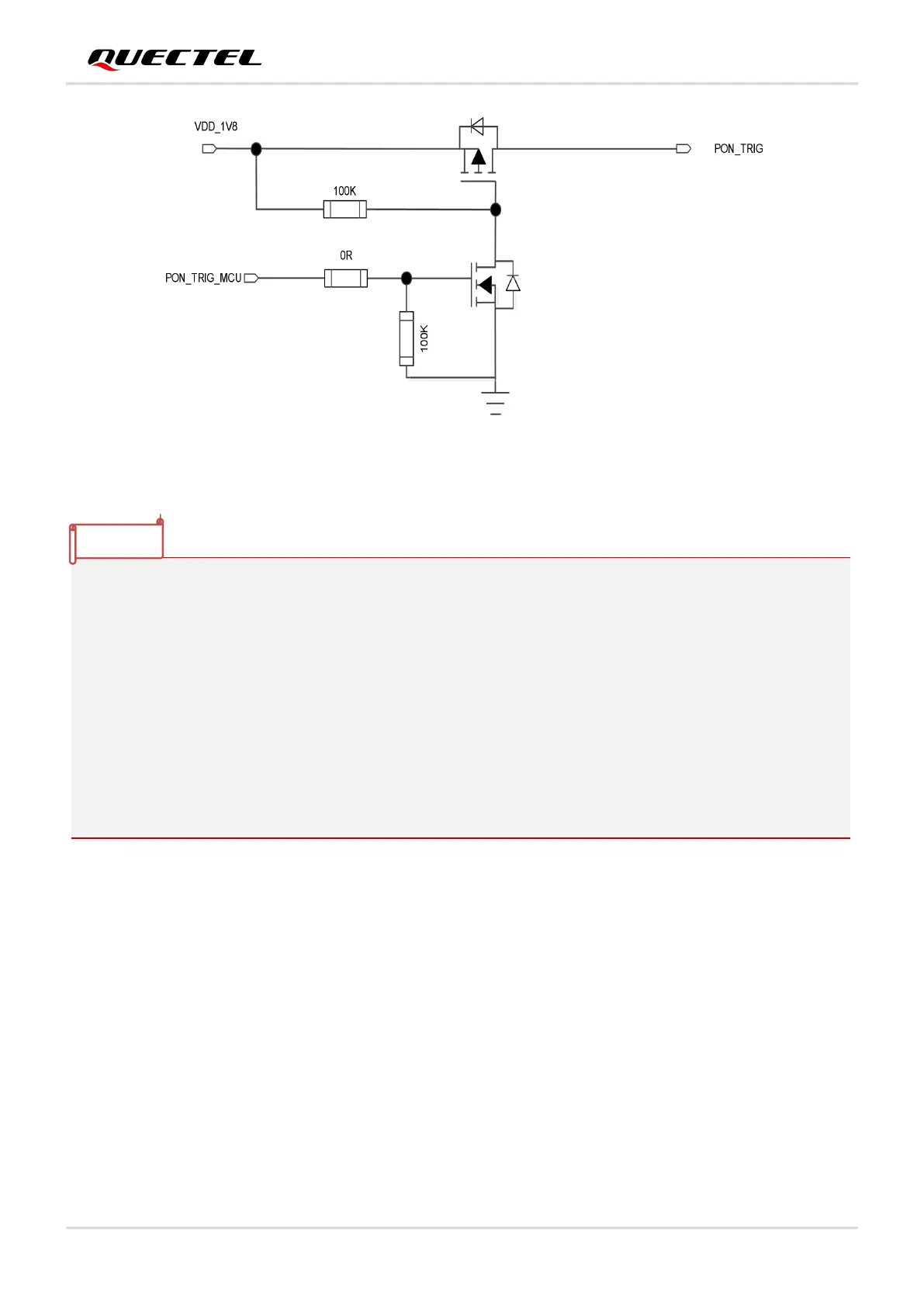
1. VDD_1V8 is provided by an external LDO.
2. The PON_TRIG pin is pulled down by default. After the module starts up, the PON_TRIG pin must be
pulled up so that the main UART interface can communicate. In normal operation mode, the
PON_TRIG pin is recommended to be pulled up all the time.
3. After sending the AT command that makes the module enter PSM mode, drive PON_TRIG low can let
the module enter PSM mode. When you need to wake up the module from PSM mode, PON_TRIG
should be pulled up all the time, otherwise the module will re-enter PSM mode.
4. Send AT+QSCLK first, and then drive PON_TRIG low after pulling down MAIN_DTR can make the
module enter sleep mode, otherwise the module cannot enter sleep mode normally. When you need
to wake up the module from sleep mode, PON_TRIG pin also should be pulled up all the time before
pulling up MAIN_DTR, otherwise the main UART interface cannot communicate.

 Loading...


