LPWA Module Series
BG950A-GL&BG951A-GL_Hardware_Design
45
/89
AT+IPR* can be used to set the baud rate of the main UART interface, and AT+IFC* can be used to set
the hardware flow control (the function is disabled by default). See document [3] for more details about
these AT commands.
Table 18: Pin Definition of Debug UART Interface
Table 19: Pin Definition of Auxiliary UART Interface
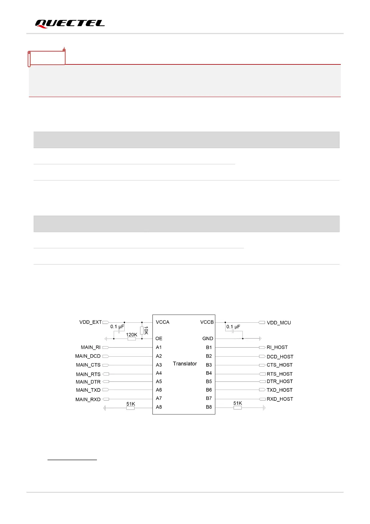
The module provides 1.8 V UART interfaces. A voltage-level translator should be used if the application
is equipped with a 3.3 V UART interface. The following figure shows a reference design of the main
UART interface:
Figure 18: Reference Circuit with Translator Chip
Visit http://www.ti.com for more information.
1.8 V power domain
If unused, keep this pin open.
Auxiliary/GNSS UART transmit
1.8 V power domain
If unused, keep this pin open.
Auxiliary/GNSS UART receive

 Loading...


