GSM/GPRS Module Series
M35 User Manual
M35_User_Manual Confidential / Released 56 / 85
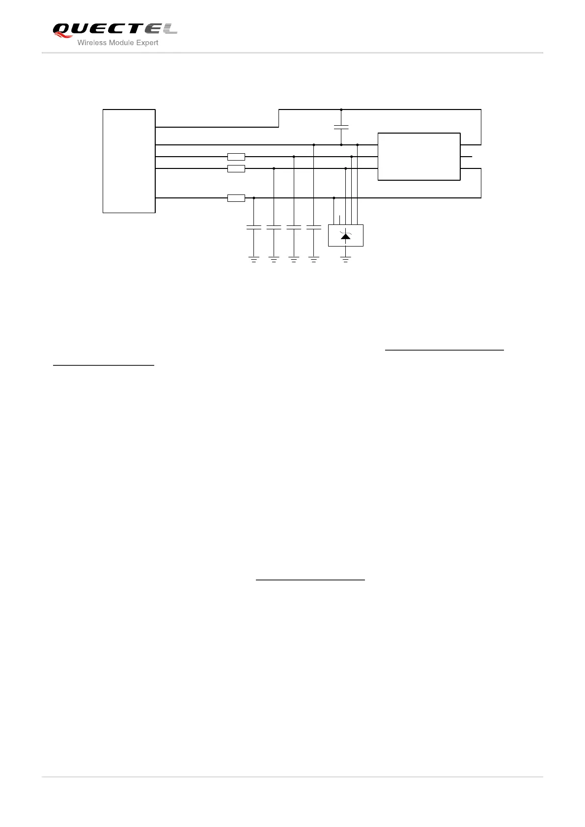
The following figure is the reference design for SIM2 interface with the 6-pin SIM card holder.
Module
SIM2_VDD
SIM_GND
SIM2_RST
SIM2_CLK
SIM2_DATA
22R
22R
22R
100nF
SIM_Holder
GND
TVS
33pF33pF 33pF
VCC
RST
CLK IO
VPP
GND
GND
33pF
Figure 35: Reference Circuit for SIM2 Interface with the 6-pin SIM Card Holder
For more information of SIM card holder, you can visit http://www.amphenol.com and
http://www.molex.com.
In order to enhance the reliability and availability of the SIM card in application. Please follow the below
criteria in the SIM circuit design.
Keep layout of SIM card as close as possible to the module. Assure the possibility of the length of the
trace is less than 200mm.
Keep SIM card signal away from RF and VBAT alignment.
Assure the ground between module and SIM cassette short and wide. Keep the width of ground no
less than 0.5mm to maintain the same electric potential. The decouple capacitor of SIM_VDD is less
than 1uF and must be near to SIM cassette.
To avoid cross talk between SIM_DATA and SIM_CLK. Keep them away with each other and shield
them with surrounded ground
In order to offer good ESD protection, it is recommended to add a TVS diode array. For more
information of TVS diode, you can visit http://www.onsemi.com/. The most important rule is to place
your ESD protection device close to the SIM card socket and make sure the net being protected will
go through the ESD device first and then lead to module. The 22Ω resistors should be connected in
series between the module and the SIM card so as to suppress the EMI spurious transmission and
enhance the ESD protection. Please to be noted that the SIM peripheral circuit should be close to the
SIM card socket.
Place the RF bypass capacitors (33pF) close to the SIM card on all signals line for improving EMI.