GSM/GPRS/GNSS Module Series
MC60 Series Hardware Design
MC60_Series_Hardware_Design Confidential / Released 68 / 114
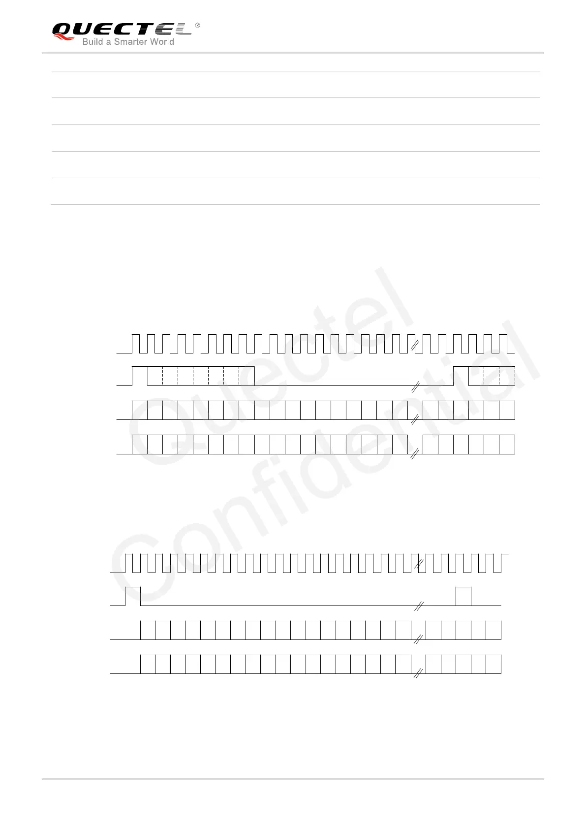
3.11.2. Timing Diagram
The sample rate of the PCM interface is 8KHz and the clock source rate is 256KHz. Every frame contains
32-bit data. The left 16 bits are valid, and the data of the left 16 bits and the right 16 bits are the same. The
following are the timing diagrams of different frame synchronization formats.
12 11 10
9 8 7 6 5 4 3 2 1 0
12 11 10 9 8 7 6 5 4 3 2 1 0
PCM_CLK
PCM_SYNC
PCM_OUT
PCM_IN
MSB
MSB
131415
15
0
15
0
131415
14
14
1
1
Figure 37: Timing Diagram for Long Frame Synchronization
PCM_CLK
PCM_SYNC
PCM_OUT
PCM_IN
12 11 10 9 8 7 6 5 4 3 2 1
0
12 11 10 9 8 7 6 5 4 3 2 1 0
MSB
MSB
131415
131415
0 15
15 1
1
0
14
14
Figure 38: Timing Diagram for Short Frame Synchronization
Module acts in master mode: 256KHz (linear)
PCM Synchronization Format
Long/short frame synchronization
 Loading...