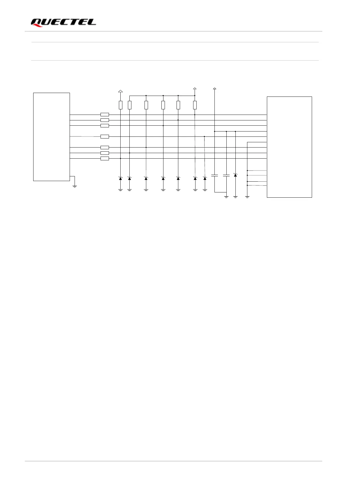
Figure 11: Reference Design of SD Card Interface
SD_VDD is a peripheral driver power supply for SD card. The maximum drive current is 600 mA. Because
of the high drive current, it is recommended to keep the trace width as at least 0.6 mm. To ensure the
stability of drive power, you should add a 4.7-μF and a 33-pF capacitor in parallel near the SD card
connector.
SD_CMD, SD_CLK and SD_DATA[0:3] are all high-speed signal traces. In PCB design, control the
characteristic impedance of these traces as 50 Ω, shield them and do not cross them with other traces. It
is recommended to route these traces on the inner layer of PCB and keep their lengths the same.
Additionally, SD_CLK needs separate ground shielding.
Layout guidelines:
⚫ Control impedance to 50 Ω ±10 %, and add ground shielding.
⚫ Trace length matching between SD_CLK and SD_CMD/SD_DATA should be less than 3 mm.
⚫ Trace length requirements: less than 150 mm when SD_CLK frequency is less than or equal to
50 MHz; less than 100 mm when SD_CLK frequency is greater than 50 MHz.
⚫ Clearance between SD card signal traces should be greater than or equal to 2 times the trace width
and the clearance between SD card signal traces and other signal traces should be greater than or
equal to 3 times the trace width.
⚫ The load capacitance requirements of SD_DATA[0:3], SD_CLK and SD_CMD traces: less than 9 pF
for SD 2.0; less than 1 pF for SD 3.0.