"
..
" .'1
LIST
OF
TABLES
Table
No.
1
2
3
4
5
6
7
8
9
10
11
SECTION 3
Data Output
Connector
Time
Base
Selection
Code
Test Equipment Required
Power Supply Resistence Measurement
Segment and
lAI Channel Decimal Point
Check
'8
1
Channel Decimal Point and
Self
Check
LF
Decimal Point
Check
rB
I
Channel Sensitivity
lA
I Channel
Sensitivity
Internal Frequency Standard
Calibration
LF
Multipl ier
Check
PARTS
LI
STS,tOMPONENT
lAYOUTS
AN
D
CIRCUIT
DIAGRAMS
C~~ponent
Layout:· Display Assembly
Parts
List
1:
Display Assembly
Page
Tech.
Spec.
(8)
T
ech.
Spec.
(9)
5-1
5-4
5-7
5-7
5-8
5-9
5-10
5-12
5-13
Fig.1
Circuit
and Component Layout:
Oscillator
Assembly Fig. 2
Parts
List
2:
Oscillator
Assembly
Parts
List
3:
Chassis, Front and Rear Panels
Parts
List
4a and 4b: Main
PCB
Assembly
Component Layout: Main
PCB
Assembly
Overall
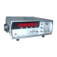
Circuit: 9916
Fig.3
Figs.4and5
SECTION 4
Parts
List
5:
LF
MultiplierAssembly
Circuit
and Component Layout:
LF
MulitiplierAssembly
Fig.6
APPENDICES
AN
D CHANGE
IN
FORM:\
rlON
9916
Vol.2
OPTION
01:
SERIAL
TO
PARALLEL
INTERFACE
UNIT Appendix 1
Cori·tents
(4)
 Loading...