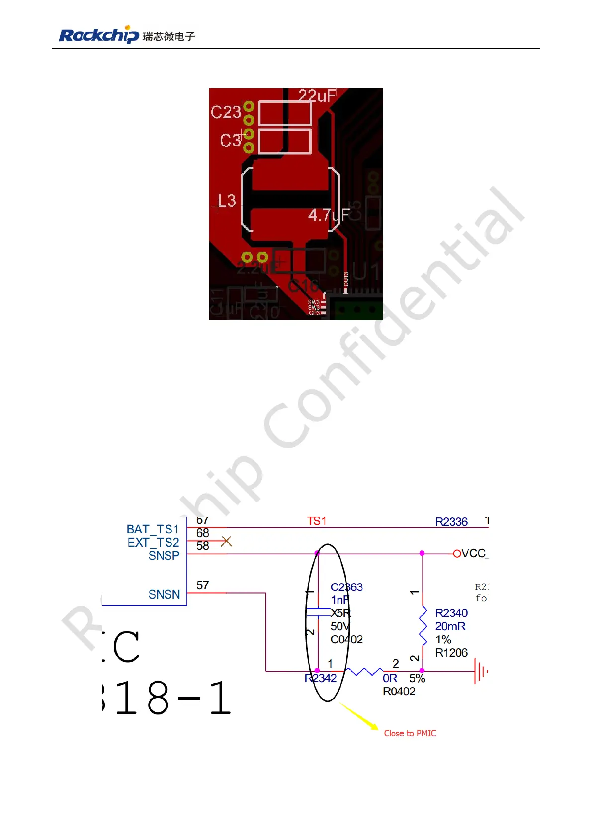
RK3288 Hardware Design Guide
Sampling point FB of DCDC should be located on the end of capacitor, don't place it on
both ends of inductor, as OUT3 trace shown in Fig 5-22.
Fig 5-22
Place charger IC close to battery to reduce internal resistance to shorten charging time.
5.5 PMIC ACT8846
There is two sample resistors in RK818, one is the current sample resistor R2340 close to
battery, and the other one is sample resistor R2342 on differential lines, as shown in Fig 5-23.
The second pin of R2342 should be placed close to the second pin of R2340, please reserve
keep-out area around R2342 and connect it to R2340 with a single node. RK2340 should be
placed close to battery. The traces of SNSP and SNSN should be compliant with differential
specification, as shown in Fig 5-24.
Fig 5-23