RK3288 Hardware Design Guide
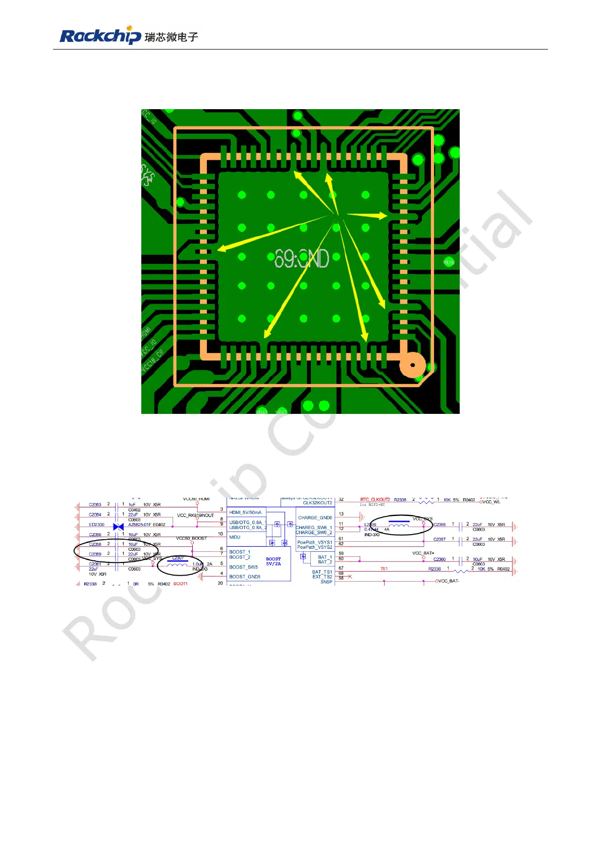
To guarantee the performance and heat dissipation of RK818, please connect it to GND
well, and the GND pins should be connected to ePAD under the chip, and enough via holes
should be placed around ePAD, as shown in Fig 5-26.
Fig 5-26
The clearance between inductors SW5 and SW6 should be more than 1.6 mm, or high
voltage caused by mutual-inductance between inductors will lead to RK818 failure. The value
of BOOST output capacitors must be more than 33uF, as shown in Fig 5-27, 5-28.
Fig 5-27