Do you have a question about the Roland SH-101 and is the answer not in the manual?
Details technical specifications of the SH-101, including keyboard, VCO, VCF, ENV, Modulator, Controller, and Sequencer.
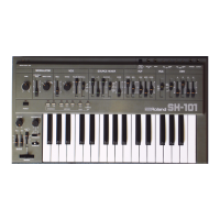
Diagram showing the top view of the SH-101 with numbered controls for identification.
Identifies internal circuit boards: Bender, Synth, Control, and Jack boards.
Functional block diagram illustrating signal flow and main modules of the SH-101.
Detailed block and connection diagram for the CEM3340 chip used in the SH-101.
Circuit diagram for the keyboard assembly, showing connections and layout.
Instructions for entering and operating the SH-101's Test Mode for adjustments and checks.
Details the Initial Set procedure, which clears RAM data but preserves sequencer data.
Describes CPU reading VCO Range, Transpose, Gate/Trig switches and outputting analog values.
CPU processing of keyboard matrix, clock signal variations, and random data generation.
CPU scanning switches, handling Load, Play, and Arpeggio modes.
CPU outputting CV data, Gate, Clock Reset, and LED illumination signals.
Diagram showing the pin connections for the TMP80C49P CPU.
Procedure for adjusting the D/A converter, covering Tune, Width (+5V), and Linearity.
Detailed steps for adjusting VCO Width, VCO Tune, and Range Width for accurate pitch.
Procedure for adjusting the VCF (Voltage Controlled Filter) cutoff frequency and width.
Instructions for adjusting the LFO (Low Frequency Oscillator) modulation offset.
Circuit and board diagram for Jack Board A, showing connections and components.
Circuit and board diagram for Jack Board B, displaying its connections and components.
Circuit and board diagram for the Bender Board, illustrating its layout and connections.
Diagram showing the MGS-1 circuit, detailing its components and connections.
Shows the component layout and foil patterns for the Control Board.
Illustrates the component layout and foil patterns for the Synth Board.
Diagram of the Switch Board, showing its circuit layout and components.
Circuit diagrams for core sound generation and shaping modules: LFO, VCO, VCF, VCA, Env Gen.
Circuit diagrams for CPU, D/A Converter, Control, and Switch boards.
Circuit diagrams for Bender board and Power Supply.
| Type | Analog Monophonic Synthesizer |
|---|---|
| Oscillators | 1 VCO |
| Envelope | ADSR |
| Keyboard | 32 keys |
| Arpeggiator | No |
| Sequencer | 100-note |
| External Control | CV/Gate |
| Year Released | 1982 |
| Waveforms | Sawtooth, Square, Pulse |
| LFO | 1 LFO |
| LFO Waveforms | Triangle, Square |
| Memory | No |
| Control | Pitch bend, Modulation |
| Outputs | Mono output, headphones |
| Power Supply | 9V DC or 6 x AA batteries |
| Sub-oscillator | Square (-1 octave) |
| Filter | 24dB/oct low-pass |