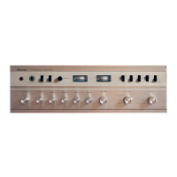
AU-X1
2.
THE
OPERATION
&
CHARACTERISTIC
OF
HIGH
SPEED
POWER
TRANSISTOR
In
order
to
up-grade
the
sou
nd
quality,
AU-Xl
employs
the
cir-
cuitry
of
the
push-pull
drive
DC
comfiguration
from
MC
head
amp
to
po
'
wer
amp
stage, which provi
de
superior
dynamic
and
open-loop
characteristics
.
The
improvement
was
made
for
parts
such
as volumes, wires, relays,
electrolytic
capacitors
and
semi-conductors.
In
particular
, newly
developed
linear high speed device, LAPT
(Linea
r
Ampl
ifier Power
Transistor)
is
adapted
in
power
stage,
and
the
combination
use
of
this
high speed
power
transistor
and
diamond
differential
circuit
allows slew
rate
of
260
V
Ills
and
wide range low
distortion
amplifi-
cation
.
2-1. High Speed Power Transistor
The
requirements
for
power
trnasistor
in
order
to
elevate
sound
quality
are;
*
to
have high cut'<lff
frequency,
fT
(high speed device).
*
to
make
voltage
dependance
of
DC
forward-current
transfer
ratio,
hFE
be little and have
excellent
linearlity.
*
to
have a large
A.5.0.
(Area
of
Safe
Operation)
and
strong
en-
durance
against
break-down
.
The
use
of
high speed
power
transisto
r
with
requirements
above
together
with
circuit
improvement
is
effective
for
achievement
of
wide range an d low
distortion
'
amplification
.
Transistors
to
meet
with
these
requirements
are
both
bi-polar and field
effect
transistor
(FET).
Note:
Cut-off
frequency,
fT
shows
the
frequency
at which
the
small signal
current
gain will be 1
(0
dB) in
common
emitter
circuit.
Comparison between bi-polar and field effect type as power
transistor.
Table
1;
Comparison
of
bi
-
polar
and field
effect
type
as a
power
device.
Field
effect
Characteristics
Bi-polar device
junc
-
MOS
FET
type
tion
type
FET
SIT
Input
impedance
low
high high
Thermal
coefficient
of
positive negative negative
operating
current
StOlied carrier
effect
exist
none none
(Carri
er
strage
effect)
Transfer
character
istic
exponential
square
square
Idring
current
as a
little large
large
output
device
Output
characteristic
pentode
triode
pentode
State
at
no
input
bias
off
on
on
Current
path
(Channel) vertical
vertical
vertical
&
horizontal
Threshold
voltage low
inter-
high
mediate
Cost
low
high high
The
advantages
of
FET
are high
input
impedance
and no
thermal
run-away because
of
negative
thermal
coefficient
of
operating
cur·
rent
however
there
still
remains
price
problem
on
FET,
in
addition,
bi-p~lar
type'
high speed
power
transistor
are variously developed
and
becoming
common
so
that
AU·X 1
employs
bi-polar
type
power
trnasistor
(LAPT).
2-2.
The
Configuration
of
High Speed Transistor
I n
order
to
increase
the
cut-off
frequency,
fT,
it
is
necessary
to
make
transistor
base as
thin
as possible,
but
it
oppose
to
A.S.O.
(Area
of
Safe
Operation)
to
enlarge. When
making
the
transistor
base
thill,
the
injected
current
density
is increased so
that
junction
is
destroied
by
second-breakdown.
To
solve above
problem,
the
con-
struction
of
power
trans
i
stor
(LAPT)
is
parallel
connection
of
devided 35
of
small signal
transistors,
in
addition,
the
defusion
resistor
is
made
at
each
emitter
of
devided
transistor
to
equalize
the
flowing
current.
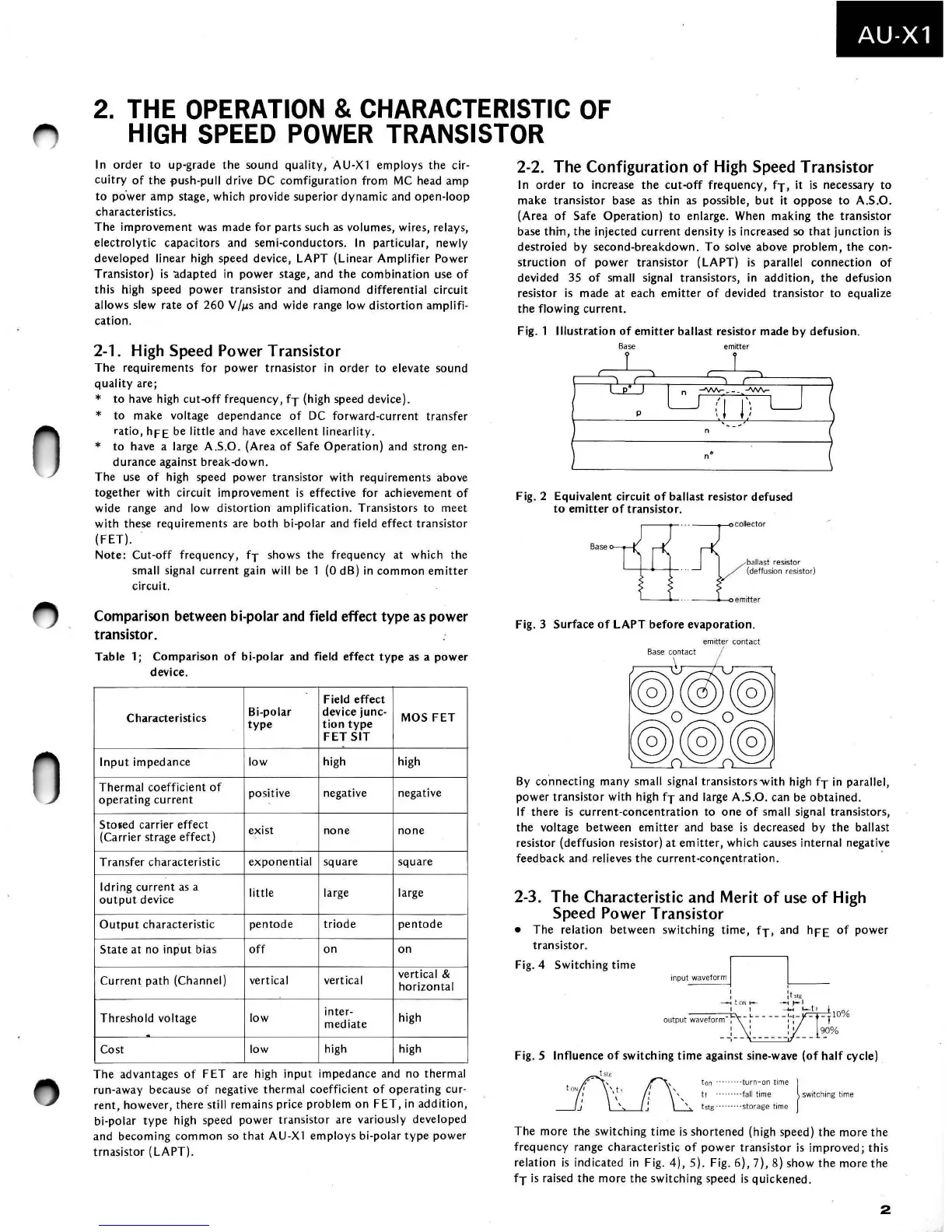
Fig. 1
Illustration
of
emitter
ballast
resistor
made
by
defusion.
B
ase
emitter
n"
Fig.2
Equivalent
circuit
of
ballast resistor
defused
to
emitter
of
transistor.
"
r§
"'
1COllecto
r
Ba
se
b
all
ast resistor
,
..
/ (
de
f
fusi
on
res
istor)
... emitter
Fig. 3
Surface
of
LAPT
before
evaporation.
e
mitt
er contact
I
By
connecting
many
small signal
transistors
with
high fT in parallel,
power
transistor
with high fT and large A.S.O. can be
obtained.
If
there
is
current-concentration
to
one
of
small signal
transistors,
the
voltage
between
emitter
and base
is
decreased
by
the
ballast
resistor
(deffusion
resistor)
at
emitter,
which causes
internal
negati~e
feedback
and relieves
the
current-con~entration.
2-3.
The
Characteristic and Merit
of
use
of
High
Speed Power Transistor
•
The
relation
between
switching
time,
fT,
and
hFE
of
power
transistor.
Fig.4
Switching
time
i
np
u
t
~
: : t
st
~
-- d
ON
t--
--
1,1
- I
t 1
~
I-
t l 0
Qu
tputwavefo
rm-
,
-
~-----:-:-
-
-T
lOYo
: : I
90%
Fig. 5
Influence
of
switching
time
against sine-wave
(of
half
cycle)
~
,_t
s
~g
..
ton
........ t
urn-ont
ime l
tON I \
tt
I
..
" \ : ".. tf ·· .. ··
··f
a
ll
t
im
e _ switching time
.J
..
~
..
tstg ·······
·st
orage t
im
e
The
more
the
switching
time
is
shortened
(high speed)
the
more
the
frequency
range
characteristic
of
power
transistor
is
improved;
this
relation
is
indicated in Fig.
4),
5).
Fig.
6),
7),8)
show
the
more
the
fT
is
raised
the
more
the
switching
speed
is
quickened.
2
 Loading...