i
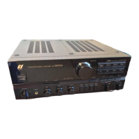
AU-X1
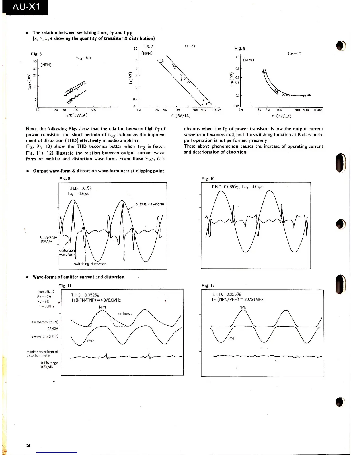
• The relation between switching time, fT and
hFE.
(x,
ll,
0,.
showing
the
quantity
of
transistor & distribution)
10
Fig. 7
Fig.
6
(NPN)
50
tstg- h
FE
(NPN)
30
i
20
'il.
2
~
.;:;
~
10
0.5
3
0.3
10
30
50
lOO
300
IM
3M
5M
hFE(5V/IA)
Next,
the
following Figs show
that
the
relation between high fT
of
power transistor and short periode
of
tstg influences the improve-
ment
of
distortion (THD) effectively
in
audio amplifier.
Fig.
9),
10)
show
the
THD becomes
better
when tstg
is
faster.
Fig.
11),
12) illustrate
the
relation between
output
current wave-
form
of
emitter
and distortion wave-form. From these Figs, it
is
• OutPl,lt wave-form & distortion wave-form near
at
clipping point.
O.l%range
IOV/div
Fig.9
T.H.D. 0.
1%
t stg =
1.6,us
I
switching distortion
• Wave-forms
of
emitter
current and distortion
(condition )
Po~
40W
Fig.
11
RL
~
8fl
.-
f ~
50KHz
lE
wa
veform (
NPN
)
2A/DIV
lE waveform( PNP)
monitor
wav
eform of
distortion meter
0.1
% range
O.5V/div
T.H
.
D.
0052%
fT(NPN/PNP) = 4.0/8.0MHz
N
PN
tf-
IT
Fig
. 8
tON
-
fT
1.0
(NPN)
0.5
\
!
0.3
5 0.2
0.1
0.05
IOM
30
M
50
M
lOOMz
IM
3M
5M
IOM
30M
SOM
lOOMz
fT(5V/IA)
fT(5V/IA)
obvious when the fT
of
power transistor
is
low
the
output
current
wave-form becomes dull, and
the
switching function
at
B class push-
pull operation
is
not
performed precisely.
These above
phenomenon
causes
the
increase
of
ope
rating current
and deterioration
of
distortion.
Fig.
10
T.H.D.
0.035%,
ts
tg
=0
.
5,us
Fig.
12
T.H.D.
0025%
fr
(NPN/PNP) = 30/21MHz
N
PN
d\A}
v
~
L-
__
___
3
______
____________
______
__________
______
__
________________________________________________
~
 Loading...