Document# SCT-UM026FVC Page 31 of 46 Confidential
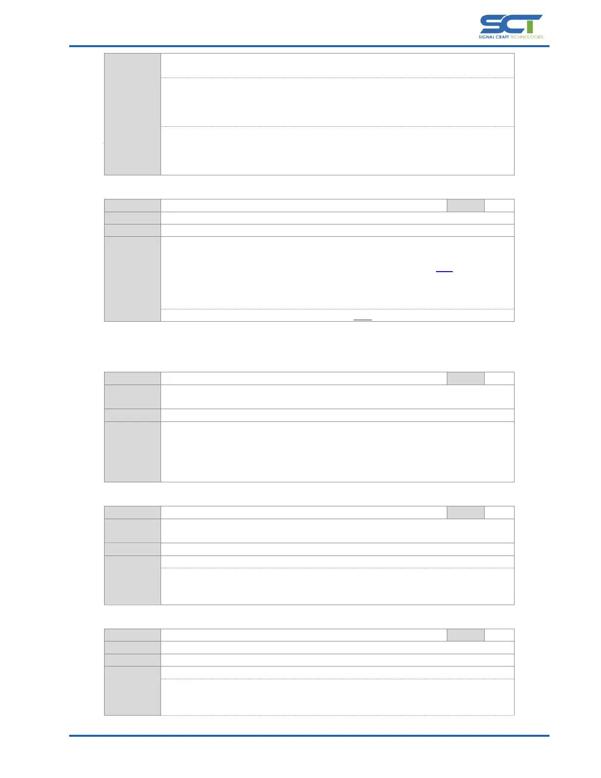
State, the binary bit position correlates to a specific GPIO pin;
i.e. bit[0] = GPIO1 … bit[7] = GPIO8
<MASK> Pin Mask:
The Pin Mask determines which GPIO pins will take on the respective bit values
contained in the Pin State.
Range = 0x00 – 0xFF
<STATE> Pin State:
Set the specified GPIO pin to either low (0) or high (1) provided that the respective bit
value is set in the Pin Mask.
Range = 0x00 – 0xFF
5.1.17 gpr
Get the state of the GPIO pins
GPIO Position Read:
Get the State of the GPIO pins as either low (0) or high (1). For GPIO pins configured
as outputs, the current state will reflect the last state set using the ‘gpw’ command.
For the returned position data, the binary bit position correlates to a specific GPIO
pin;
i.e. bit[0] = GPIO1 … bit[7] = GPIO8
Returned read data can be accessed using the ‘read’ command.
5.2 RFFE Commands
5.2.1 clock
Set the SCLK frequency. By default, the clock is set to 26000 kHz. Once set, the actual
frequency achieved is confirmed.
<FREQ> Clock Frequency:
Specify the clock frequency in kilohertz.
Range = 100 – 60000 kHz
5.2.2 hsdr
Set the RFFE Half Speed Data Response
Halves the clock rate during slave responses to register read commands.
<ENABLE> Half Speed Data Response:
0 = Disable (full speed)
1 = Enable (half speed)
5.2.3 rr
Perform an RFFE Register Read operation
<SA> Slave Address:
Address of the RFFE Slave device to communicate with.
Range = 0-15

 Loading...