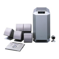
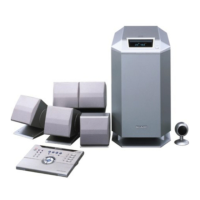
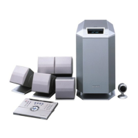
HT-CN150DVW
73
Name Pin Numbers I/O Definition
UDAC 115 O Video DAC ouput
YUV0 O YUV pixel 0 output data.
TWS 116 O Audio transmit frame sync output.
SEL_PLL2 I System and DSCK output clock frequency selection is made at the rising
edge of RESET#. The matrix below lists the available clock frequencies and
their respective PLL bit settings. Strapped to VCC or ground via 4.7 kΩ resis-
tor, reading during reset.
TSD0
117
O Audio transmit serial data port 0.
SEL_PLL0 I Refer to the description and matrix for SEL_PLL2 pin 116.
TSD1
118
O Audio transmit serial data port 1.
SEL_PLL1 Refer to the description and matrix for SEL_PLL2 pin 116.
TSD [2:3] 120, 121 O Audio transmit serial data ports 2 and 3.
MCLK 122 I/O Audio master clock for audio DAC.
TBCK 123 O Audio transmit bit clock.
SPD_DOBM 124 O S/PDIF output.
SEL_PLL3 I
Clock source select. Strapped to VCC or ground via 4.7 kΩ resistor, read only
during reset.
F : CVBS/Chroma signal for simultaneous mode.
Y : Luma component for YUV and Y/C processing.
C : Chrominance signal for Y/C processing.
U : Chrominance component signal for YUV mode.
V : Chrominance component signal for YUV mode.
PIN 109 110 113 114 115
Value F DAC V DAC Y DAC C DAC U DAC
0 CVBS/Chroma CVBS1 Y C N/A
1 CVBS/Chroma CVBS1 Y C CVBS2
2 CVBS/Chroma N/A Y C N/A
3 CVBS/Chroma CVBS1 N/A N/A CVBS2
4 CVBS/Chroma CVBS1 N/A N/A N/A
5 CVBS/Chroma CVBS1 Y Pb Pr
6 CVBS/Chroma N/A Y Pb Pr
7 N/A SYNC G B R
8 CVBS/Chroma Chroma Y Pb Pr
9 CVBS CVBS1 G B R
10 CVBS CVBS1 G R B
11 N/A SYNC G R B
12 CVBS/Chroma N/A Y Pr Pb
13 CVBS/Chroma CVBS1 Y Pr Pb
14 Chroma Y G R B
SEL_PLL2 SEL_PLL1 SEL_PLL0 Clock Type (MHz)
0 0 0 CLK X 4.5
0 0 1 CLK X 5.0
0 1 0 BYPASS
0 1 1 CLK X 4.0
1 0 0 CLK X 4.25
1 0 1 CLK X 4.75
1 1 0 CLK X 5.5
1 1 1 CLK X 6.0
SEL_PLL3 Clock Source
0 Crystal oscillator
1 CLK input