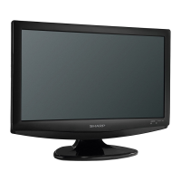
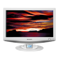
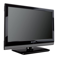
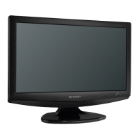
LC-19D1E/S-BK/WH
5 – 21
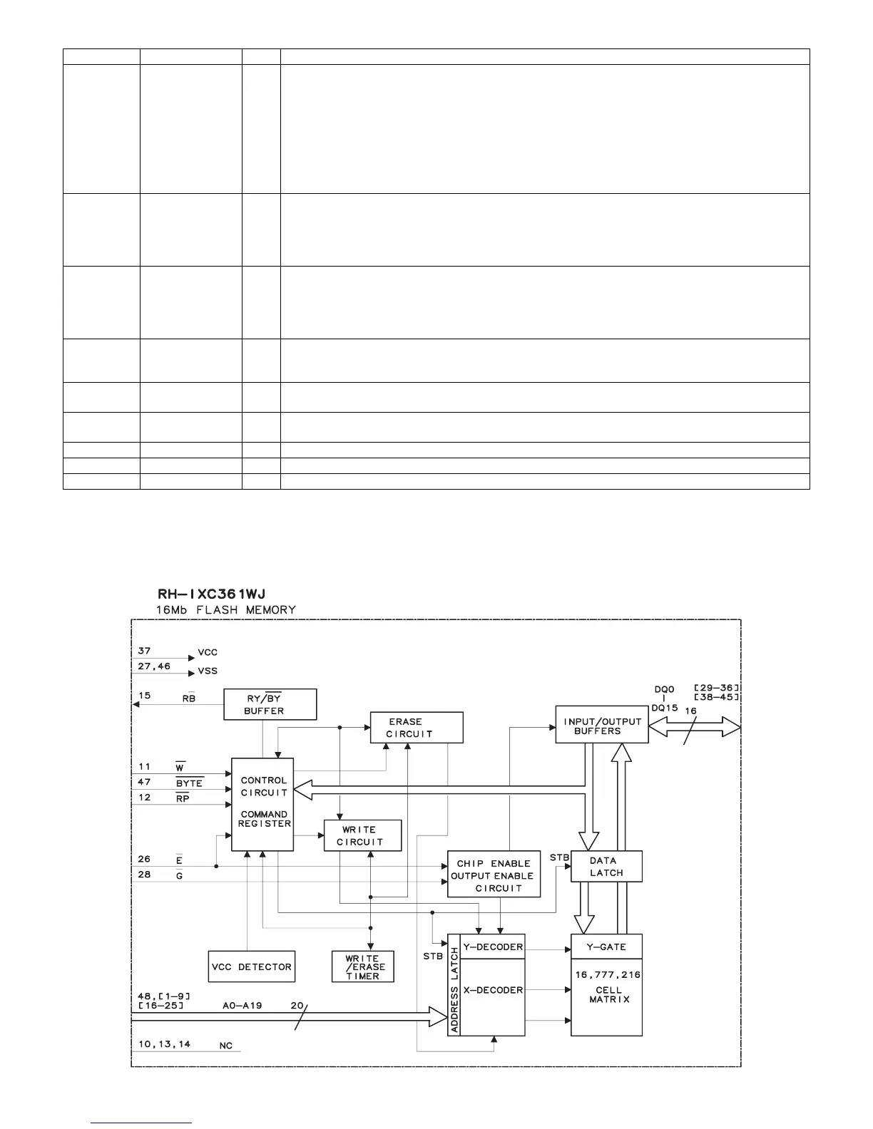
2.12. IC4202 (RH-iXC361WJZZ)
2.12.1 Block Diagram
28-32, 35-42 A [0 : 12] I Address Inputs : Provide the row address for ACTIVE commands, and the column address and AUTO
PRECHARGE bit for READ/WRITE commands, to select one location out of the memory array in the
respective bank.
A10 is sampled during a PRECHARGE command to determine whether the PRECHARGE applies to
one bank (A10 LOW) or all banks (A10 HIGH).
If only one bank is to be precharged, the bank is selected by BA0, BA1.
The address inputs also provide the op-code during a MODE REGISTER SET command.
BA0 and BA1 define which mode register is loaded during the MODE REGISTER SET command (MRS
or EMRS).
2, 4, 5, 7, 8,
10, 11, 13,
54, 56, 57,
59, 60, 62,
63, 65
DQ I/O Data Input/Output : Data bus.
16,51 LDQS,(U)DQS I/O Data Strobe : Output with read data, input with write data.
Edge-aligned with read data,centered in write data.
Used to capture write data.
For the x16, LDQS corresponds to the data on DQ0~D7 ; UDQS corresponds to the data on
DQ8~DQ15
14, 17, 19,
25, 43, 50,
53
NC - No Connect : No internal electrical connection is present.
3, 9, 15, 55,
61
VDDQ - DQ Power Supply : +2.5V ± 0.2V. (+2.6V ± 0.1V for DDR400)
6, 12, 52,
58, 64
VSSQ - DQ Ground.
1, 18, 33 VDD - Power Supply : +2.5V ± 0.2V. (+2.6V ± 0.1V for DDR400)
34, 48, 66 VSS - Ground.
49 VREF SSTL_2 reference voltage.
Pin No. Pin Name I/O Pin Function