39
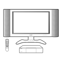
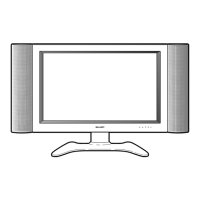
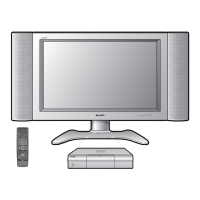
LC-30HV4E
» Pin mapping
Pin No. Pin Name Type Description
63 TV I Video signal input
1 V1 I Composite video signal input
8V2 I
15 V3 I
22 V4 I
30 V4 I
60 V4 I
3 Y1 I Y/C separation signal input, used for luminance signal input
10 Y2 I YIN1: Input for signal created by Y/C separation of VOUT1 output
17 Y3 I
24 Y4 I
49 YIN1 I
5 C1 I Y/C separation signal input, used for chrominance signal input
12 C2 I CIN1: Input for signal created by Y/C separation of VOUT1 output
19 C3 I
26 C4 I
51 CIN1 I
62, 2 LTV, LV1 I Audio signal input
9, 16 LV2, LV3 I
23, 29 LV4, LV5 I
59, 64 LV6, RTV I
4, 11 RV1, RV2 I
18, 25 RV3, RV4 I
31, 61 RV5, RV6 I
53 VOUT1 O Video signal output, used for composite vide signal output
41 VOUT3 O
44 V/YOUT2 O Video signal output, controlled via I2C bus and used for composite video signal output
56 YOUT1 O Power or luminance signal output is selected.
39 YOUT3 O Video signal output, used for luminance signal output
58 COUT1 O Video signal output, used for chrominance signal output
47 COUT2 O
37 COUT3 O
52 LOUT1 O Audio signal output
43 LOUT2 O
38 LOUT3 O
54 ROUT1 O
45 ROUT2 O
40 ROUT3 O
6 S2-1 I Used for detection of S2-compatible DC that is superimposed to C signal.
13 S2-2 I 4:3 image signal is selected when voltage less than 1.3V, 4:3 letterbox signal when
20 S2-3 I 1.3V or more 2.5V or less, and 16:9 squeeze signal when voltage less than 2.5V. 4:3
27 S2-4 I image signal is selected when the pins are open because they are pulled down to
GND via 100kΩ.
7 S-1 I Used for selection between composite video signal and S signal.
14 S-2 I Detection result is written to the status register. S signal is selected when voltage more
21 S-3 I than 3.5V, and composite video signal when voltage less than 3.5V. Composite video
28 S-4 I signal is selected when the pins are open because they are pulled down to 5V via
100kΩ.
32 ADR I Used for selection of slave address for I2C bus.
90H is selected when voltage less than 1.5V, and 92H when more than 2.5V.
90H is selected when the pin are open.
33 SCL I I2C bus signal input
34 SDA I I2C bus signal input
36 DC OUT O Used for output of S2-compatible DC that is superimposed to COUT3.
DC superimposition is done by connecting to COUT3 via capacitor. The pin is
controlled via I2C bus.
Connection of 4.7kΩ external resistor provides output impedance of 10±3kΩ that
conforms to S2.
55 TRAP1 I Connected to trap circuit for sub carrier.
46 TRAP2 I
48 MUTE I Mute for audio signal output.
Mute is on when voltage less than 1.3V and off when voltage more than 2.5V.
Mute is off when the pin is open.
50 BIAS I Internal reference bias input.
Connected to GND via capacitor.