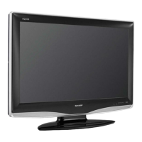
LC32D44E/S/RU-BK/GY (1st Eddition)
5 – 15
Programmable I/O pins
127 POI0[7] I/O PIO PORT 0
126 PIO0[6]
123 PIO0[5]
122 PIO0[4]
121 PIO0[3]
120 PIO0[2]
119 PIO0[1]
118 PIO0[0]
46 PIO1[7] I/O PIO PORT 1
45 PIO1[6]
44 PIO1[5]
43 PIO1[4]
41 PIO1[3]
40 PIO1[2]
39 PIO1[1]
38 PIO1[0]
117 PIO2[7] I/O PIO PORT 2
116 PIO2[6]
115 PIO2[5]
114 PIO2[4]
111 PIO2[3]
110 PIO2[2]
109 PIO2[1]
108 PIO2[0]
12 PIO3[6] I/O PIO PORT 3
11 PIO3[5]
10 PIO3[4]
7 PIO3[3]
6 PIO3[2]
5 PIO3[1]
4 PIO3[0]
JTAG test access port (TAP) pins
134 TDI I TAP boundary scan test data input.
133 TMS I TAP boundary scan test mode select.
137 TCK I TAP boundary scan test clock.
135 NOT_TRST I TAP boundary scan test logic reset.
132 TDO O TAP boundary scan test data output.
DCU pins
1 DCUTRIGGERIN I External trigger input to DCU.
2 DCUTRIGGEROUT O Signal to trigger external debug circuitry.
Analog power supply pins (Audio DAC)
32 VDDAADAC --- 3.3v power for audio DAC.
31 GNDAADAC --- Ground for audio DAC.
30 VSSUBANA --- Substrate ground for all DACs.
Analog power supply pins (Video DAC)
22 VDDDAC0 --- 3.3 V power supply for video DAC 1, 2 and 3.
21 VDDDAC1 --- 3.3 V power supply for CVBS video DAC 4.
19 VSSDAC0 --- Ground for video DAC 1, 2 and 3.
20 VSSDAC1 --- Ground for video DAC 4.
Analog power supply pins (Frequency synthesizers)
140 VDDDFS1 --- Frequency synthesizer 1.2 V digital power dedicated to frequency synthesizer 1.
141 GNDDFS1 --- Frequency synthesizer 1.2 V digital ground dedicated to frequency synthesizer 1.
142 VCCAFS --- Frequency synthesizer 1.2 V analog power shared between frequency synthesizer
1 and 2.
143 GNDAFS --- Frequency synthesizer 1.2 V analog ground shared between frequency synthe-
sizer 1 and 2.
144 GNDDFS2 --- Frequency synthesizer 1.2 V digital ground dedicated to frequency synthesizer 2.
145 VDDDFS2 --- Frequency synthesizer 1.2 V digital power dedicated to frequency synthesizer 2.
Analog power supply pins (PLLs)
146 VCCAPLL --- 1.2V PLL1 analog power.
147 GNDAPLL --- 1.2V PLL1 analog ground.
148 GNDAPLL1 --- 1.2V PLL2 analog ground.
149 VCCAPLL1 --- 1.2V PLL2 analog power.
Analog power supply pins (LMI SDRAM)
Pin No. Pin Name I/O Pin Function


