Wide 4.75V to 23V Operating Input Range
Output Adjustable from 1.22V to 21V
Under-Voltage Lockout
15.3. Pinning
1 BOOT High-Side Gate Drive Bootstrap Input. BS supplies the drive for the
high-side N-Channel MOSFET switch.
2
IN Power Input. Drive IN with a 4.75V to 23V power source.
3
SW Power Switching Out is the switching node that supplies power to the
output
4
GND Ground.
5
FB Feedback Input. FB senses the output voltage and regulates it. Drive
FB with a resistive voltage divider from the output voltage. FB
threshold is 1.222V.
6
COMP Compensation Node is used to compensate the regulation control
7
EN Enable/UVLO. A voltage greater than 2.71V enables operation. For
complete low current shutdown the EN pin voltage needs to be at less
than 900mV. When the voltage on EN exceeds 1.2V, the internal
regulator will be enabled and the soft-start capacitor will begin to
charge. The MP1583 will start switching after the EN pin voltage
reaches 2.71V.
8
SS Soft-Start Control Input. SS controls the soft-start period.
16. FDC642
16.1. General Description
This P-Channel 2.5V specified MOSFET is produced using Fairchild’s advanced
PowerTrench® process that has been especially tailored to minimize on-state resistance
and yet maintain low gate charge for superior switching performance.
These devices have been designed to offer exceptional power dissipation in a very small
footprint for applications where the larger packages are impractical.
16.2. Features
Max rDS(on) = 65 mΩ at VGS = -4.5 V, ID = -4.0 A
Max rDS(on) = 100 mΩ at VGS = -2.5 V, ID = -3.2 A
Fast switching speed
Low gate charge (11nC typical)
High performance trench technology for extremely low rDS(on)
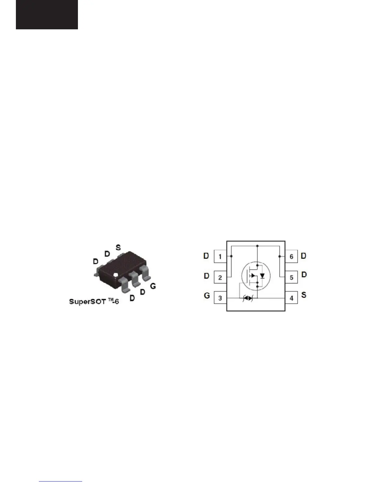
SuperSOTTM-6 package: small footprint (72% smaller than standard SO-8);
low profile (1 mm thick)
Termination is Lead-free and RoHS Compliant
16.3. Pinning
17. FDC604P
17.1. General Description
This P-Channel 1.8V specified MOSFET uses Fairchild’s low voltage PowerTrench
process. It has been optimized for battery power management applications.
17.2. Features
–5.5 A, –20 V. RDS(ON) = 33 mΩ @ VGS = –4.5 V
RDS(ON) = 43 mΩ @ VGS = –2.5 V
RDS(ON) = 60 mΩ @ VGS = –1.8 V
Fast switching speed.
High performance trench technology for extremely low RDS(ON)(S)
17.3. Pinning