77
INSTRUCTION FETCH
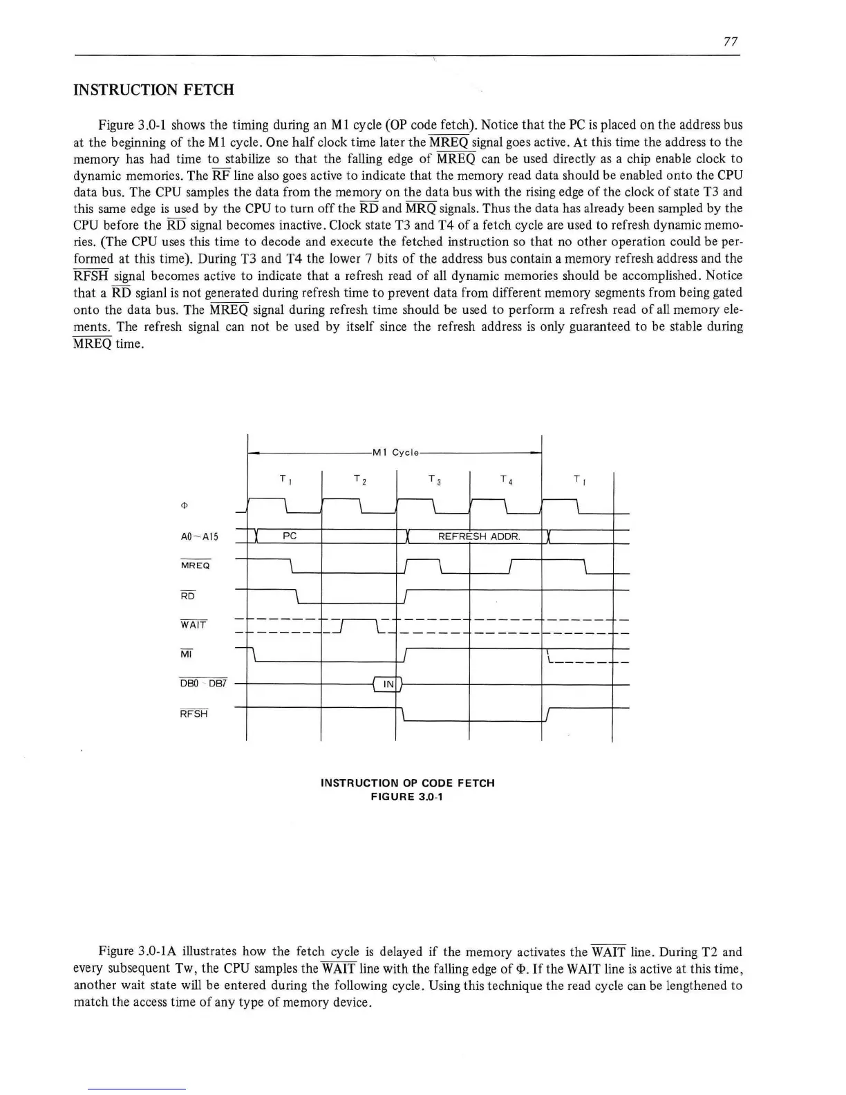
Figure 3.0-1 shows the timing during an
Ml
cycle (OP code fetch). Notice
that
the
PC
is
placed
on
the address bus
at the beginning
of
the
Ml
cycle. One half clock time later the MREQ signal goes active. At this time the address to the
memory has had time
to
stabilize
so
that
the falling edge
of
MREQ can be used directly
as
a chip enable clock
to
dynamic memories. The RF line also goes active to indicate that the memory read data should be enabled onto the CPU
data bus. The CPU samples the data from the memory
on
the data bus with the rising edge
of
the clock
of
state T3 and
this same edge
is
used by the CPU
to
turn
off the RD and MRQ signals. Thus the data has already been sampled by the
CPU
before the RD signal becomes inactive. Clock state T3 and
T4
of
a fetch cycle are used
to
refresh dynamic memo-
ries. (The CPU uses this time
to
decode and execute the fetched instruction so that no other operation could be per-
formed at this time). During T3 and
T4
the lower 7 bits
of
the address bus contain a memory refresh address and the
RFSH signal becomes active to indicate that a refresh read
of
all dynamic memories should be accomplished. Notice
that a RD sgianl
is
not generated during refresh time
to
prevent data from different memory segments from being gated
onto
the data bus. The MREQ signal during refresh time should be used
to
perform a refresh read
of
all
memory ele-
ments. The refresh signal can not
be
used by itself since the refresh address
is
only guaranteed
to
be stable during
MREQ time.
T ,
-
~
y
PC
MREQ
\
\
-
,_
_____
r-------
-
1\
DBO
DB?
M
I
Cycle
T z
T 3 T 4
~
~
IL-
X
REFRESH
ADDR.
I
I
_-y-c_
------
------
------
------
I
'ii\lr-c
L:.:...:.fl
\
INSTRUCTION
OP
CODE
FETCH
FIGURE
3.0-1
T l
~
X
\
------
-
------
-
\_
_____
-
I
Figure
3.0-lA
illustrates how the fetch cycle
is
delayed if the memory activates the
WAIT
line. During T2 and
every subsequent Tw, the
CPU samples the
WAIT
line with the falling edge
of
<I>.
If
the WAIT line
is
active at this time,
another wait state will be entered during the following cycle . Using this technique the read cycle can be lengthened to
match the access time
of
any type
of
memory device.