78
-J
-
AO
-
A15
MREQ
RD
DBO
087
-
Ml
-
WAIT
-
RFSH
Ml
Cycle
Tl
T2
T w
T w T 3
T4
~
~
~
~
~
~
IY
PC
X
REFRESH
ADDR.
\
\
I
r-;;:;
~~
1\
I
-----
1-""l_L--
=}___J._-=-
-_r---c-
------
------
r--
--
- -
------
\
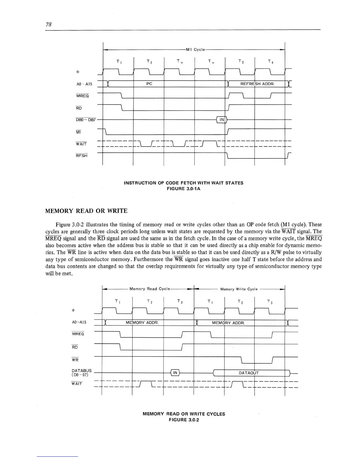
INSTRUCTION
OP
CODE
FETCH
WITH
WAIT
STATES
FIGURE
3.0-1A
I
------
r-------
MEMORY READ
OR
WRITE
,---
X
-
Figure 3.0-2 illustrates the timing
of
memory read or write cycles other than an
OP
code fetch
(M
1 cycle). These
cycles are generally three clock periods long unless wait states are requested by the memory
via
the WAIT signal. The
MREQ signal and the RD signal
are
used the same
as
in the fetch cycle. In the
case
of
a memory write cycle, the MREQ
also becomes active when the address bus
is
stable
so
that it can
be
used directly
as
a chip enable for dynamic memo-
ries. The
WR
line
is
active when data
on
the data bus
is
stable
so
that it can be used directly
as
a R/W pulse
to
virtually
any type
of
semiconductor memory. Furthermore the
WR
signal goes inactive one half T state before the address and
data bus contents are changed so
that
the overlap requirements for virtually any type
of
semiconductor memory type
will be met.
AO
-
AI5
MREQ
RD
WR
DATABUS
(
D0
- 0
7)
WAIT
Memory
Read
Cycle
Mem
ory
Writ
e Cycle
T l
T 2 T 3
T l
T 2 T 3
---'
~
~
~
~
~
~
X
MEMORY
ADDR.
X
MEMORY
ADDR.
\ I
\_
I
\ I
\ I
IN
DATAOUT
-
1-----
r-.TL~
-----
-----
1-_-Jl.~
------
--
-----
1------
------
MEMORY
READ
OR
WRITE
CYCLES
FIGURE
3.0-2
-----
r---
L_
---