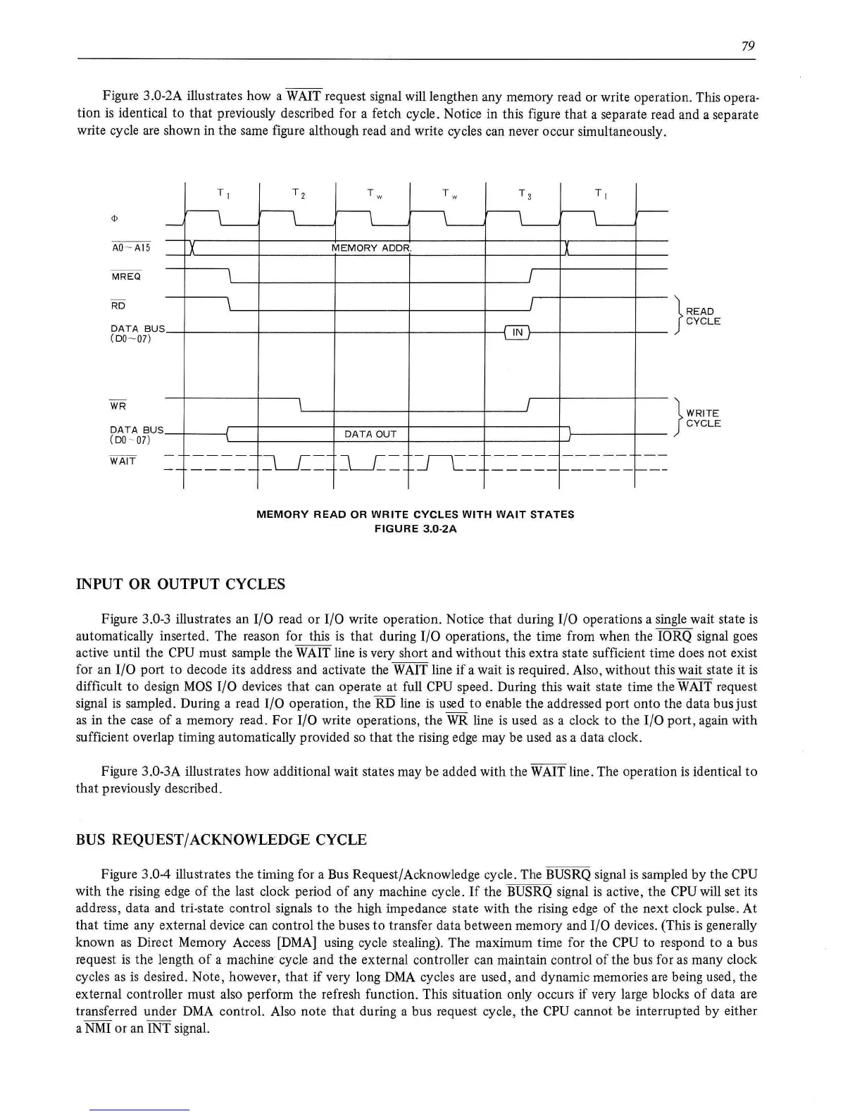
79
Figure 3.0-2A illustrates how a WAIT request signal will lengthen any memory read or write operation. This opera-
tion
is
identical to that previously described for a fetch cycle. Notice in this figure that a separate read and a separate
write cycle are shown in the same figure although read and write cycles can never occur simultaneously.
~
-
AO
-
AI5
MREQ
RD
DATA
BUS
(
D0
- 07)
WR
DATA
BUS
(DO
- 07)
WAIT
-
--
T l
T2
T w T w
T3
T,
~
r---L-
~
r---L-r---L-r---L-
X
~
\
-----
-----
MEMORY
ADDR.
X
I
I
IN
~
J
DATA
OUT
~--
l___L=
TL~
-----
-----
-
---
-----
------
MEMORY
READ
OR
WRITE
CYCLES
WITH
WAIT
STATES
FIGURE
3.0-
2A
INPUT OR OUTPUT CYCLES
lr----
--
---
}
READ
CYCLE
}
WRITE
CYCLE
Figure 3.0-3 illustrates an
I/0
read or
I/0
write operation. Notice that during
I/0
operations a single wait state
is
automatically inserted. The reason for this
is
that during
I/0
operations, the time from when the IORQ signal goes
active until the
CPU must sample the WAIT line
is
very short and without this extra state sufficient time does not exist
for an
I/0
port
to
decode its address and activate the
WAIT
line
if
a wait
is
required. Also, without this wait state it
is
difficult
to
design
MOS
I/0
devices that can operate at full CPU speed. During this wait state time the
WAIT
request
signal
is
sampled. During a read
I/0
operation, the RD line
is
used
to
enable the addressed port onto the data bus just
as
in the
case
of
a memory read.
For
I/0
write operations, the
WR
line
is
used
as
a clock to the
I/0
port, again with
sufficient overlap timing automatically provided
so
that
the rising edge may be used
as
a data clock.
Figure
3.0-3A illustrates how additional wait states may be added with the WAIT line. The operation
is
identical
to
that previously described.
BUS REQUEST/ACKNOWLEDGE CYCLE
Figure 3.0-4 illustrates the timing for a Bus Request/Acknowledge cycle. The BUSRQ signal
is
sampled
by
the CPU
with the rising edge
of
the last clock period
of
any machine cycle.
If
the BUSRQ signal
is
active, the CPU will set its
address, data and tri-state control signals to the high impedance state with the rising edge
of
the next clock pulse. At
that
time any external device can control the buses
to
transfer data between memory and
I/0
devices. (This
is
generally
known
as
Direct Memory Access
[DMA]
using cycle stealing). The maximum time for the CPU to respond
to
a bus
request
is
the length
of
a machine cycle and the external controller can maintain control
of
the bus for
as
many clock
cycles
as
is
desired. Note, however, that if very long
DMA
cycles are used, and dynamic memories
are
being used, the
external controller must also perform the refresh function. This situation only occurs if very large blocks
of
data are
transferred under
DMA
control. Also note that during a bus request cycle, the CPU cannot be interrupted by either
a
NMI
or an INT signal.