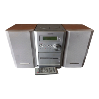
XL-30H/30W
– 44 –
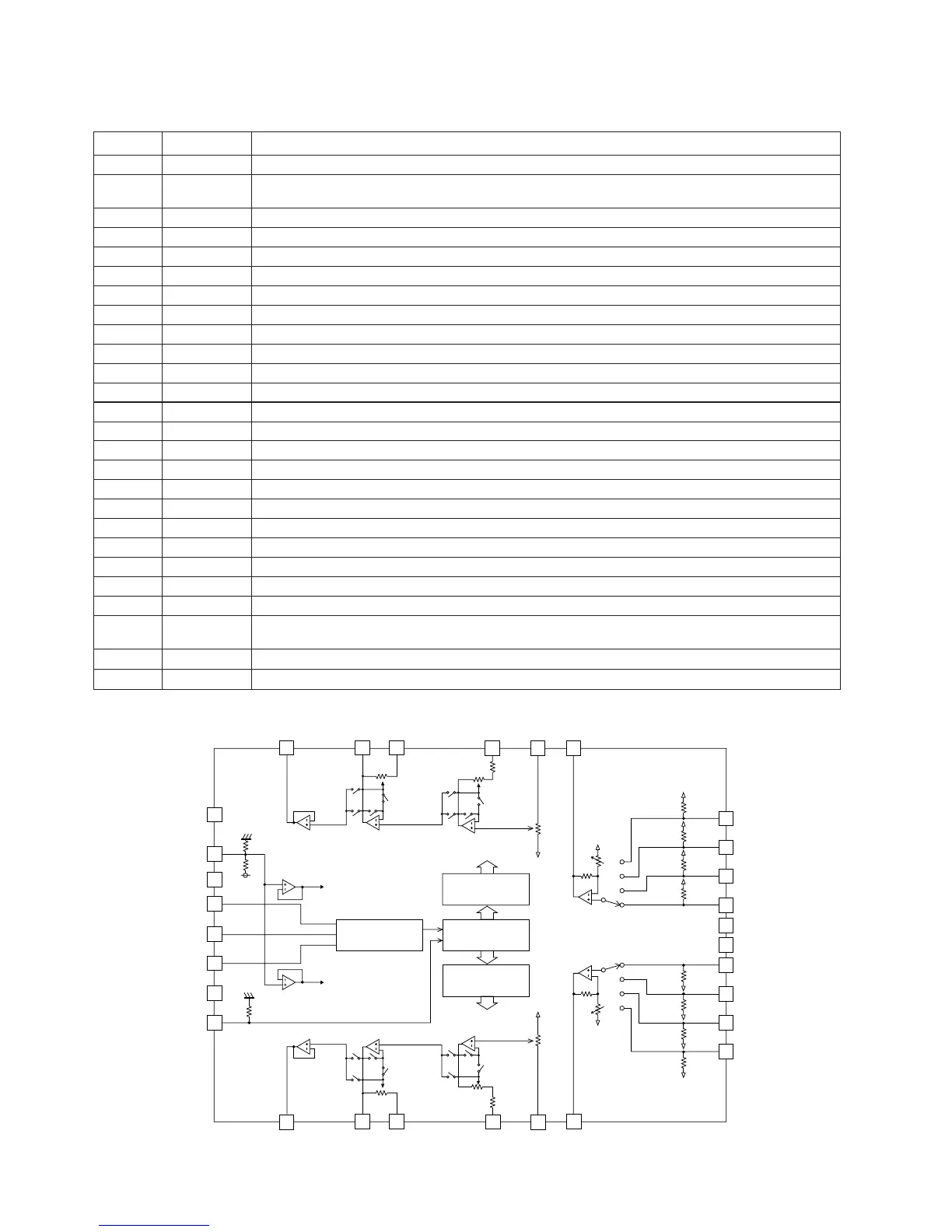
FUNCTION TABLE OF IC
IC401 VHiLC75342M-1: Function/Volume Equalizer (LC75342M)
1 DI Serial data and clock input pin for control.
2 CE Chip enable pin. Data written into an internal latch in a timing of [H] -> [L]. Each analog switch is activated.
Data transfer enabled at [H] level.
3 VSS Ground pin.
4 TEST Electronic volume control pin. To be set to the VSS potential.
5 LOUT Volume + equalizer output pin.
6 LBASS2 Bass-band filter comprising capacitor and resistor connection pin.
7 LBASS1 Bass-band filter comprising capacitor and resistor connection pin.
8 LTRE Capacitor connection pin comprising treble band filter.
9 LIN Volume + equalizer input pin.
10 LSEL0 Input selector output pin.
11* L4 Input signal pin.
12-14 L3-L1 Input signal pin.
15* NC No CONNECT pin. To be open or connected to VSS.
16* NC No CONNECT pin. To be open or connected to VSS.
17-19 R1-R3 Input signal pin.
20* R4 Input signal pin.
21 RSEL0 Input selector output pin.
22 RIN Volume + equalizer input pin.
23 RTRE Capacitor connection pin comprising treble band filter.
24 RBASS1 Bass-band filter comprising capacitor and resistor connection pin.
25 RBASS2 Bass-band filter comprising capacitor and resistor connection pin.
26 ROUT Volume + equalizer output pin.
27* NC No CONNECT pin. To be open or connected to VSS.
28 Vref 0.5 x VDD voltage generation block for analog ground. Capacitor of several 10µF to be connected between
Vref and AWSS (VSS) as a counter measure against power ripple.
29 VDD Supply pin.
30 CL Serial data and clock input pin for control.
Pin No. Port Name Function
In this unit, the terminal with asterisk mark (*) is (open) terminal which is not connected to the outside.
Figure 44 BLOCK DIAGRAM OF IC
6
7
8910
11
12
13
14
15
16
17
18
19
20
212223
24
25
26
5
27
28
30
29
1
2
3
4
LVref
RVref
CCB
INTERFACE
CONTROL
CIRCUIT
LOGIC
CIRCUIT
CONTROL
CIRCUIT
ROUT
RBASS1
RBASS2
RTRE
RIN
RSEL0
L1
L2
L3
L4
R1
R2
R3
R4
LOUT
LBASS2
LBASS1
LTRE
LIN
LSEL0
VSS
CE
DI
CL
VDD
NC
Vref
NC
NC
TEST