XV-Cl
E
l
BRIGHT
(pin No. 43)
Used to receive DC voltage for brightness adjustment.
l
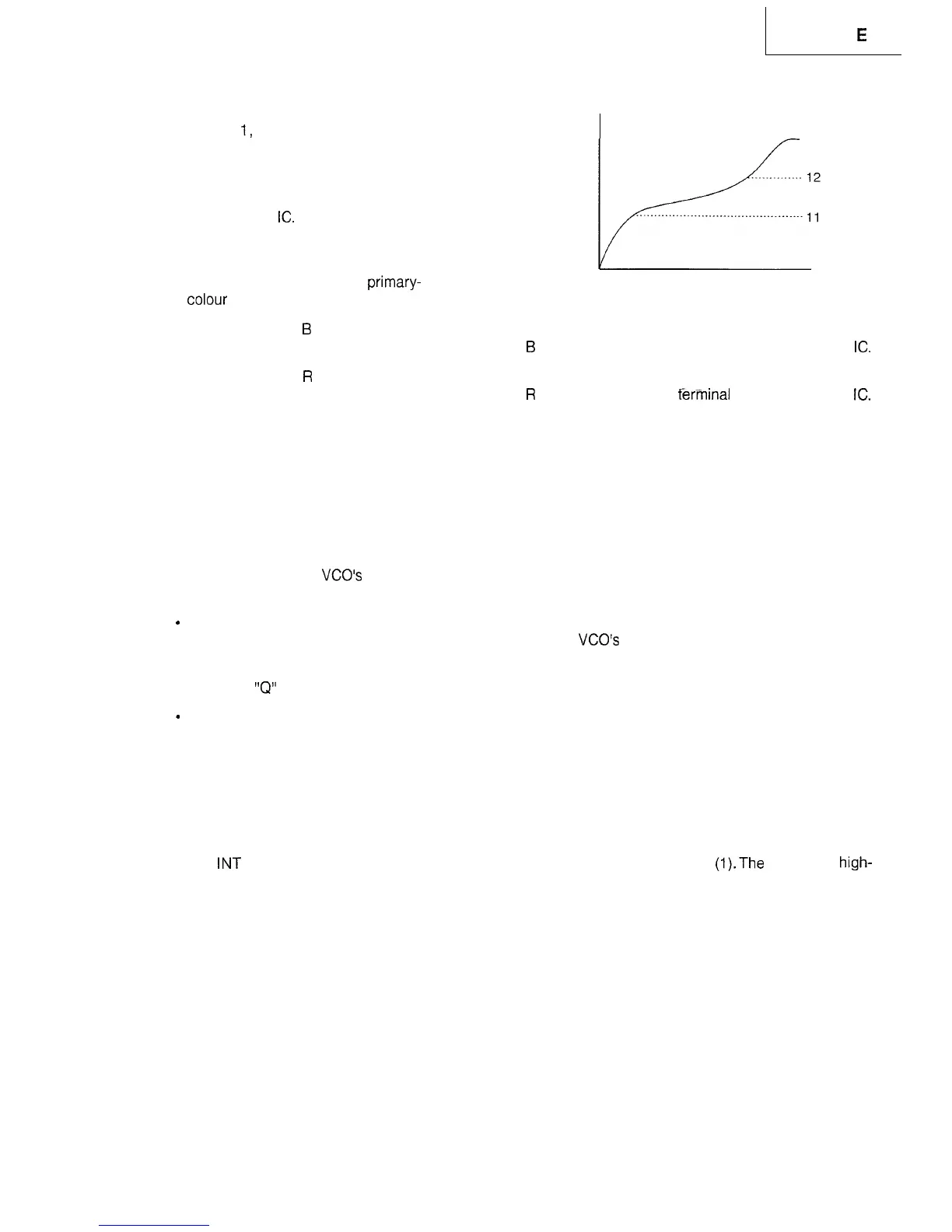
GAMMA
1,
GAMMA 2 (pin Nos. 44 and 45)
Used to receive DC voltage to set a
gamma-correction DC voltage gain
switching point. (See the figure at
right.) The Gamma 2 terminal is pre-
set inside the
IC.
output
PEAK
LIMITER
l
PEAK LIMITER (pin No. 46)
Used to receive DC voltage to set the
white peak limiter level for
primary-
colour output.
Input
l
SUB CONTRAST
B
(pin No. 47)
Used to receive DC voltage for fine adjustment of the
B
signal’s contrast. This terminal is preset inside the
IC.
l
SUB CONTRAST
R
(pin No. 48)
Used to receive DC voltage for fine adjustment of the
R
signal’s contrast. This ferminal is preset inside the
IC.
ii) Circuit behavior
l
ACC detector, ACC amplifier
They form an ACC loop and serve to detect the peak of the burst signal amplitude.
l
VCO, APC detector
The VCO local oscillation circuit is of Pierce crystal oscillator type and functions as a crystal unit. The APC
detector phase-detects the burst signal and the VCO oscillation output signal. The resulting detection voltage
is used to control the VCO’s oscillation frequency and to form a phased-locked loop. By doing so, no readjust-
ment is needed.
9
Killer detector
The detector is used to phase-detect the burst signal and the
VCO’s
oscillation output signal.
l
Picture adjustment circuit
The value
“Q”
of the luminance signal delay line is changed in order to adjust the frequency characteristic.
*
AGC circuit
Various AGC characteristics can be achieved depending on the luminance signal’s APL. The luminance
signal is fed to the filter at pin (17) to get rid of the high-frequency components. The resulting signal goes to
the AGC detector to detect the peak.
l
Filter adjustment
The resistance between pin (12) and GND can be regulated to adjust the filter’s frequency characteristic.
l
External input switch
The
INT
and EXT signals can be switched over by the control signal coming to pin
(l).The
switch is of
high-
speed type.
27