Table 11: Characteristic data of the digital outputs
Type Switching
Switching behavior PNP switching against supply voltage V
S
Properties Short-circuit protected
Temperature protected
Not electrically isolated from V
S
Electrical values The electrical values are identical for all digital outputs.
0 V ≤ V
out
1)
≤ V
S
(V
S
2)
−1.5 V) ≤ V
out
≤ V
S
at I
out
3)
≤ 100 mA
1)
Output voltage.
2)
Supply voltage.
3)
Output current.
V
out
3
4
Digital output 1
!
"
Signal 2
GND
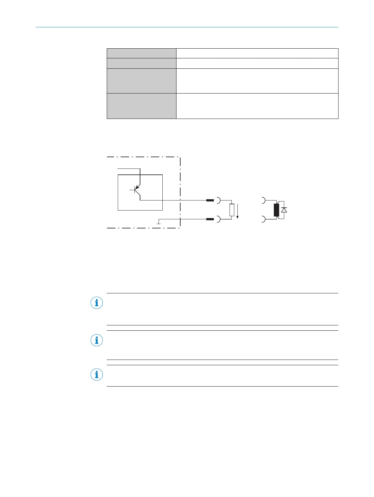
Figure 26: Wiring a digital output on the device
1
Digital output
2
Output signal
3
Output voltage V
out
4
With inductive load: see note
!..."
For pin assignment, see respective device
NOTE
Provide an arc-suppression switch at the digital output if inductive load is present.
b
Attach a freewheeling diode directly to the load for this purpose.
NOTE
Capacitive loads on the digital outputs have an effect on the switch-on and switch-off
behavior. The limit value is a maximum capacitance of 100 nF.
NOTE
The digital outputs are not suitable for time-critical applications.
1. Connect the digital outputs according to the application.
2. For the thorough check of the switching functions, use a high resistance digital
voltmeter and wire the digital outputs with a load.
This prevents the display of incorrect voltage values/output states.
External digital outputs in the CDB/CDM connection module (optional):
The optional CMC600 parameter cloning module provides two additional external digi‐
tal outputs at the corresponding terminals in the connection module.
ELECTRICAL INSTALLATION 6
8017840/19OF/2021-10-28 | SICK O P E R A T I N G I N S T R U C T I O N S | CLV61x
45
Subject to change without notice