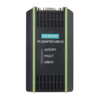
Hardware Design of the PC Adapter USB
PC Adapter USB
A5E01134250-01
4-5
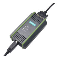
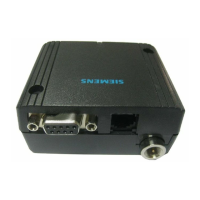
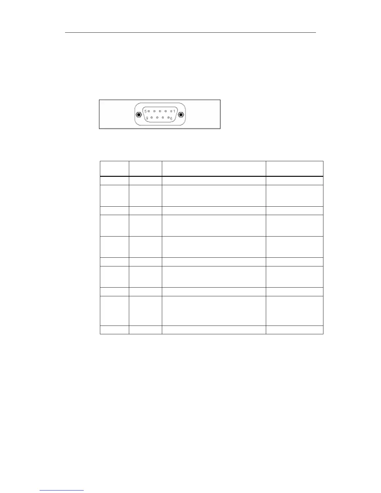
4.4 MPI/DP interface
Pin assignment
Pin assignment of the MPI/DP interface:
Description of signals
Pin no. Short name Meaning Input /
Output
1 NC Not connected –
2 M24V Zero volt of the 24 V power supply,
provided by the electronic DC/DC circuit of
the adapter (AS potential range)
Input
3 LTG_B Data line B Input / Output
4 RTS_AS RTSAS control signal for receive data
current. The signal is active ‘1’ when the
directly connected AS is transmitting data.
Input
5 M5V Reference potential of the MPI/DP
interface for the RTS_AS and RTS_PG
signals
Input
6 P5V Not connected
7 P24V Zero volt of the +24 V power supply,
provided by the electronic DC/DC circuit of
the adapter (AS potential range)
Input
8 LTG_A Data line A Input / Output
9 RTS_PG Adapter’s RTS output signal. The signal is
‘1’ when the adapter is transmitting data.
The signal is not contained in the 0.3 m
MPI cable!
Output
Shielding on connector housing*
* The shielding is interconnected with the USB interface via the adapter electronic module.