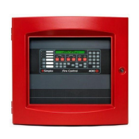
2-6
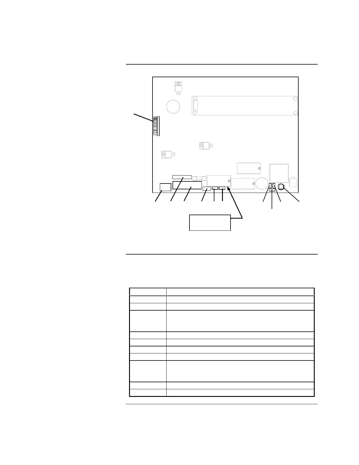
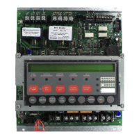
Figure 2-3. 565-325 Master Controller PCB Assembly
Table 2-2 describes the I/O connectors on the Master Controller PCB Assembly
(refer to Figure 2-2 for the location of these connectors).
Table 2-2. 565-325 Master Controller PCB Assembly I/O Connectors
Label Description
TB1 External Comm, City Circuit, Trouble Circuit
SW1 Reset Switch
JW1 – JW2 Selects U18 size
•
JW
1-
OUT
, JW2-
OUT
: 2 Meg
•
JW
1-
OUT
, JW2-
IN
: 4 Meg
P1 Keypad connector
P2 Power / Comm Connector to Slave
P3 CFIG Download Programmer Port
P4 City Circuit Jumpers
P5 CFIG Flash Programming Jumper
• Enable Flash Programming – 1-2
• Disable Flash Programming – 2-3
P6 Carrier Detect TXD Enable (1-2 Normal, 2-3 Modem)
P7 RAM Battery Jumper (normally 1-2)
Continued on next page
4020 Master Controller,
Continued
Master Controller PCB Layout
Master Controller PCB
Assembly I/O Connectors
JW2
JW1
SW1