Sinclair ZX Spectrum Service Manual
Spectrum For Everyone https://spectrumforeveryone.com/
10
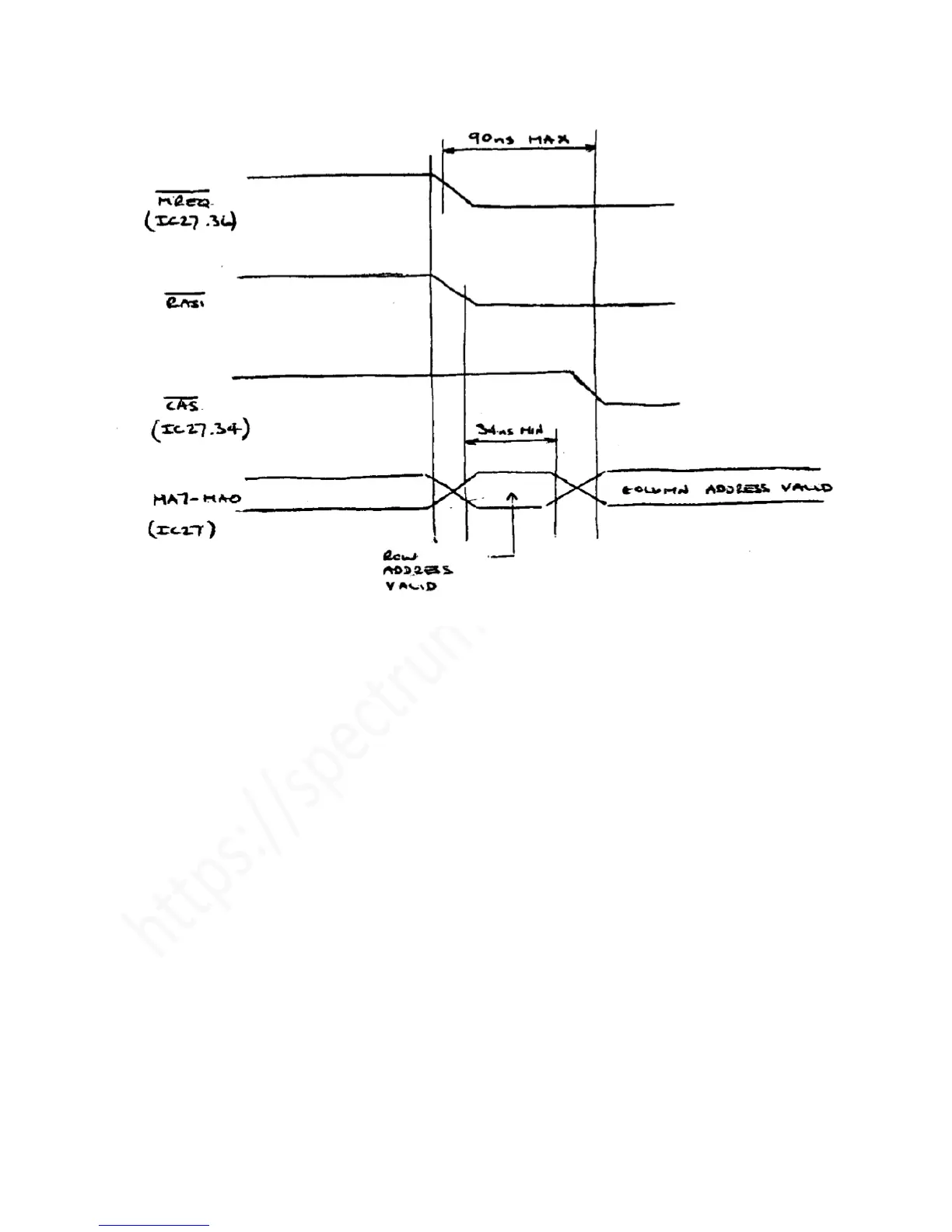
Figure 1.2. Uncontended RAM RAS/CAS timing (read cycle shown)
Resistors R1 to R8, in series with the data bus lines, perform a similar function to the address port
resistors described above. They ensure that the ULA does not 'see' CPU write data while the ULA is
accessing the contended RAM.
Refresh for the contended RAM is accomplished during normal read cycles, i.e. most rows are refreshed
each time the ULA accesses screen pages during picture compilation; the remaining rows are refreshed
as a result of other read cycles also known to occur at regular intervals within the refresh period.
Bank Register (IC31): The bank register is at address 7FFD
H
in the Z80 address space. The register is
positive edge triggered and latches D5-D0 off the data bus on the negative (trailing) edge of the BANK
output from the PAL IC29. BANK is decoded (set high) from /IORQ and RD/WR active low (I/O read or
write cycle) and ZA1 and ZA15 low (address 7FFD
H
).
On selecting the 48K Spectrum mode, the Z80 writes a ‘1’ into bit 5 of the register, thus preventing any
further access. This action preserves the Z80 address space, preventing erroneous calls to address 7FFD
H
crashing the SPECTRUM program. The bit can only be cleared by using the RESET pushbutton or by
interrupting the power supply input.
 Loading...