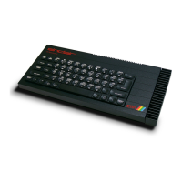
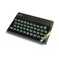
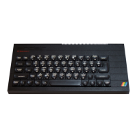
Sinclair ZX Spectrum Service Manual
Spectrum For Everyone https://spectrumforeveryone.com/
11
1.5 INPUT/OUTPUT
The input/output functions are controlled by the Z80 in conjunction with the ULA (IC1) and the sound
generator circuit IC32. Like its counterpart in the 48K Spectrum, the ULA handles the tape recorder
read/write functions, and generates an interrupt during which it scans the main keyboard. It also
accesses the contended RAM area while generating the drive waveforms for the TV display and
produces a simple tone output while obeying the BEEP instruction.
The sound generator produces high quality music sound by mixing the outputs from up to three
programmable tone generators and a noise generator. It also handles the RS232/MIDI interface and
reads the keypad status. Each of these functions and the supporting circuits is described below.
1.5.1 TV Picture Generation and Sound Output
The video compilation section of the ULA operates in conjunction with the memory mapped picture
display area in the contended RAM, together with the colour encoder IC36 and UHF modulator. This
combination produces a high resolution 24 line x 32 character, eight colour display suitable for use with
RGB colour or black and white monitors or a domestic TV receiver. The sound output from the ULA or
the programmable sound generator is FM modulated and added to the composite video signal for
playback through the TV loudspeaker. If a monitor is used the sound is available through the MIC socket.
From the 17.73 MHz external clock (X1/IC37) the ULA derives line and field timing for the composite
sync signal on pin 23, and a pixel clock for timing accesses to the RAM. The ULA also generates two 8.8
MHz clocks on pins 46, 47 from which the encoder derives the 4.43 MHz reference and quadrature
chroma sub-carriers. The fact that the pixel and chroma carriers are derived from the same external
clock source means that dot crawl is eliminated. The dot pattern itself is minimised by adjusting the
display line length.
The digital RGB and bright-up signals available from the ULA on pins 19-22 are derived by accessing the
picture information located in page 5 or 7 of the contended RAM area at the pixel rate (para. 4.12.8).
The addresses are necessarily independent of the CPU and appear on the ULA address lines DMA6 to
DMA0 and DMA7 as two separate bytes, timed by the RAS/CAS row/column address select lines. DMA7
is a decode of bit 3 (VB) loaded in the bank register IC31 and sets the most significant row/column
address bits as follows:
 Loading...