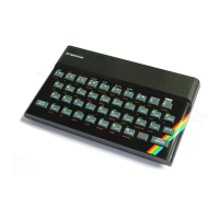
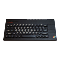
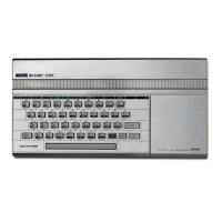
Sinclair ZX Spectrum Service Manual
Spectrum For Everyone https://spectrumforeveryone.com/
9
An external ROM chip select input, supplied via the expansion port on pin 25A, selectively disables the
on-board ROM by pulling the select input high. By virtue of R33 placed on the ULA side of the ROM the
ULA /ROMCS output is effectively inhibited. Interface 1 uses this mechanism, allowing the CPU to read
the extension ROM in the interface for microdrive and RS232 applications.
Uncontended RAM (IC15-22): The uncontended RAM comprises eight 64K dynamic RAM chips
organised as a 64K byte memory with a 256 x 256 row/column matrix. When ULA15 is high (see para.
4.11) separate 8-bit row/column addresses are supplied by IC27 as MA7-MA0. These are derived from
the Z80 address bus A13-A0 with UA14 and UA15 from IC29. The low order address bits A6-A0 with
UA14 provide the row address and are selected at the beginning of the memory access cycle when
initially the /RAS (/MREQ) output from the Z80 is low. Later, as the row address is latched, IC27 asserts
/CAS selecting the high order address bits A13-A7 with UA15.
Row/column address selection and RAS/CAS timing for the RAM is decoded in IC27 in conjunction with
IC28 and the associated discrete components. A theoretical timing diagram illustrating the RAS/CAS
waveforms is given in Figure 1.2 (A read operation is shown when the WRL line from the Z80 is high).
Contended RAM (IC6-13): The organisation of the contended and uncontended RAM described above is
identical. However, because ULA15 is low during accesses to the contended area, IC27 only sources a 7-
bit row/column address DMA6-DMA7. The most significant address bit is sourced by the 2:1 data
selector IC30. At the start of the memory access cycle IC1 asserts /DRAS and selects the row address as
A13-A7 off the Z80 address bus with VA14 via the selector. Later as the row address is latched IC1 sets
/DRAS and selects the column address as A6-A0 with VA15.
RAS/CAS timing for the contended RAM area is decoded by the ULA IC1 from /MREQ and A15. /DCAS is
asserted a short time after /DRAS returns high, and latches the column address. ULA15 prevents IC27
generating an identical signal for the uncontended RAM. The /DRAMWE signal, also generated by the
ULA, is a decode of the RD/WR waveforms and selects a RAM read or RAM write cycle.
It will be apparent from the circuit diagram that the ULA can access the contended RAM by generating a
set of addresses independent of those generated by the CPU. The address port for the RAM is therefore
dualled by the insertion of small value series resistors on the address lines between IC27 and the RAM.
This ensures that where there is likely to be conflict between the ULA and CPU, the ULA address has
priority. Priority is assigned on the basis that the ULA must access screen pages 5 and 7 at set intervals in
order to build up the video for the TV display. If the ULA is about to access the RAM and it detects either
A14 or A15 (i.e. the CPU is also about to access the RAM) the ULA inhibits the CPU clock temporarily
halting the CPU memory transaction until its own transaction is completed.
 Loading...