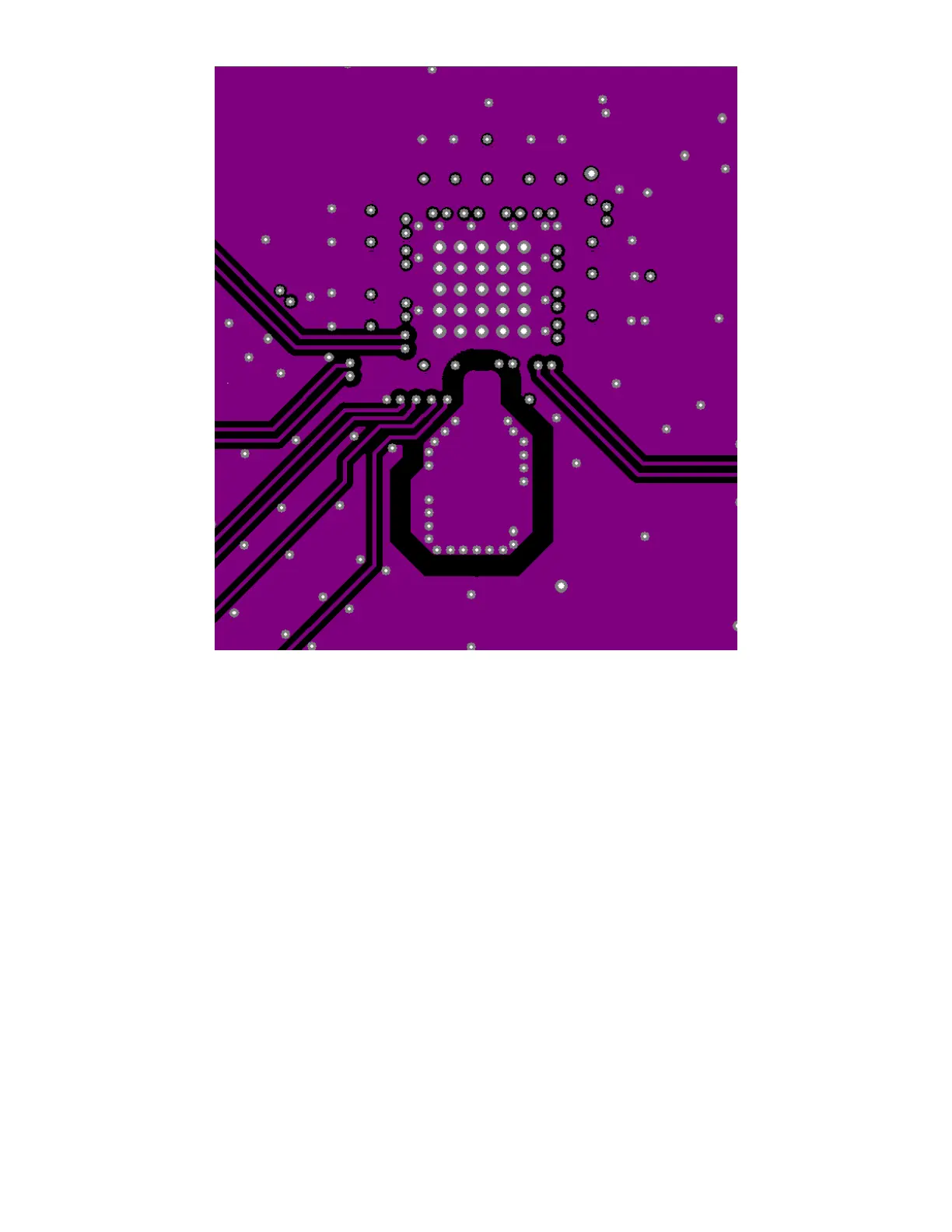
Figure 12.2. Zoom View Crystal Shield Layer, Below the Top Layer (Layer 2)
Figure 12.2 Zoom View Crystal Shield Layer, Below the Top Layer (Layer 2) on page 53 shows the layer that implements the shield
underneath the crystal. The shield extends underneath the entire crystal and the X1 and X2 pins. This layer also has the clock input
pins. The clock input pins go to layer 2 using vias to avoid crosstalk. As soon as the clock inputs are on layer 2, they have a ground
shield above, below, and on the sides for protection.
Figure 12.3 Crystal Ground Plane (Layer 3) on page 54 is the ground plane and shows a void underneath the crystal shield. Figure
12.4 Power Plane (Layer 4) on page 55 is a power plane and shows the clock output power supply traces. The void underneath the
crystal shield is continued.
Si5391 Reference Manual • Crystal, XO and Device Circuit Layout Recommendations
Skyworks Solutions, Inc. • Phone [781] 376-3000 • Fax [781] 376-3100 • sales@skyworksinc.com • www.skyworksinc.com
53 Rev. 0.5 • Skyworks Proprietary Information • Products and Product Information are Subject to Change Without Notice • January 11, 2022 53
 Loading...