EasyManua.ls Logo

Sony CDX-51 - Page 62

Sony CDX-51
68 pages
Print Icon
To Next Page IconTo Next Page
To Previous Page IconTo Previous Page
Loading...
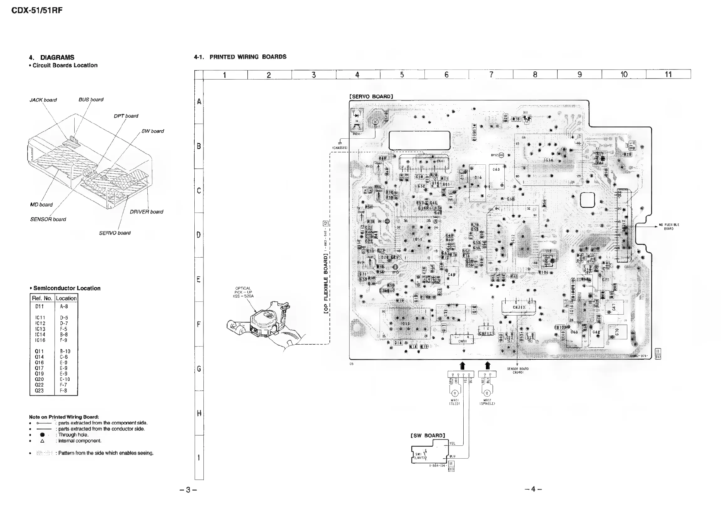
CDX-51/51RF
4.
DIAGRAMS
4-1,
PRINTED
WIRING
BOARDS
*
Circuit
Boards
Location
1
2
ied]
2.
05:
Aaa
oe
A
et
eet
|
ae
10
1
YACK
board
ate
ad
A
5
2
B
|
Cc
MD
board
/
7
/
|
y)
|
DRIVER
board
/
SENSOR
board
/
S
nes
/
04RD
SERVO
board
D
¢
-
a
<
9
rs)
E 4
*
Semiconductor
Location
gerteaL,
2
sbctath
bernie
dently
Z
%
Ref.
No.
|Location
KSS
~
5208
Z
Dit
AB
6
IC11
0-5
112
0-7
F
1013
F-5
1C14
B-8
IC16
F-9
ones
Qn
8-10
|
m7]
Qt4
C-6
1
iu)
Q16
E-9
j
6
ai7
E-9
Qi9
E-9
Q20
E-10
Q22
F-7
023
F-8
soe
(PINOLE!
|H
Note
on
Printed
Wiring
Board:
*
o——
:
parts
extracted
from
the
component
side.
*
——
‘parts
extracted
from
the
conductor
side.
*
@
—
:
Through
hole.
*
A:
intemal
component.
. :
Pattern
from
the
side
which
enables
seeing.
|
Tecate:
|!
i}