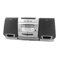
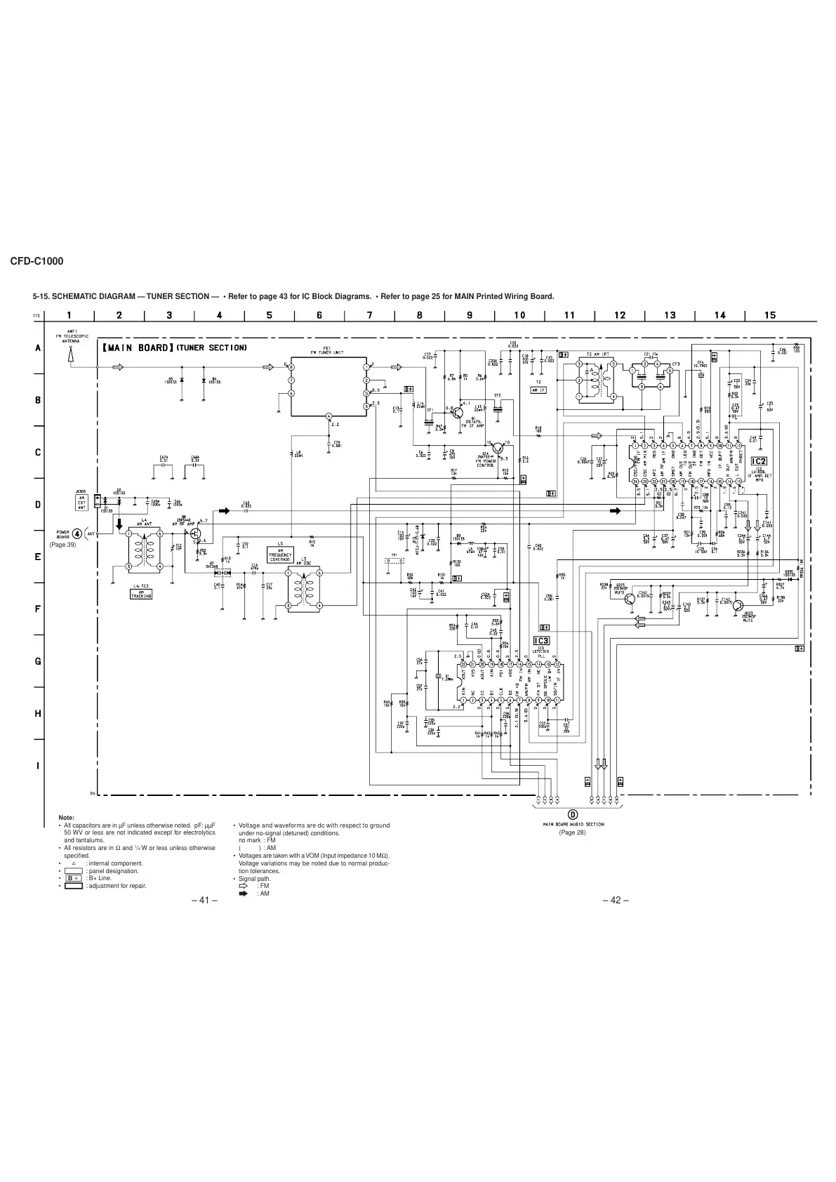
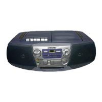
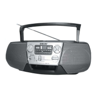
CFD-C1000
– 41 – – 42 –
5-15. SCHEMATIC DIAGRAM — TUNER SECTION — • Refer to page 43 for IC Block Diagrams. • Refer to page 25 for MAIN Printed Wiring Board.
Note:
• All capacitors are in µF unless otherwise noted. pF: µµF
50 WV or less are not indicated except for electrolytics
and tantalums.
• All resistors are in Ω and
1
/
4
W or less unless otherwise
specified.
•
¢
: internal component.
• C : panel designation.
• U : B+ Line.
• H : adjustment for repair.
115
• Voltage and waveforms are dc with respect to ground
under no-signal (detuned) conditions.
no mark : FM
( ) : AM
• Voltages are taken with a VOM (Input impedance 10 MΩ).
Voltage variations may be noted due to normal produc-
tion tolerances.
• Signal path.
F : FM
f : AM
(Page 39)
(Page 28)