1111
D-FS601
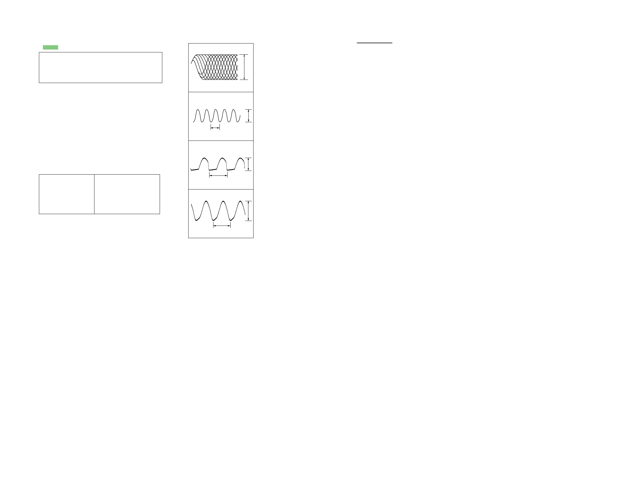
• Waveforms
Note on Printed Wiring Board:
• X : parts extracted from the component side.
• : Pattern from the side which enables seeing.
Note on Schematic Diagrams:
• All capacitors are in µF unless otherwise noted. pF: µµF
50 WV or less are not indicated except for electrolytics
and tantalums.
• All resistors are in Ω and
1
/
4
W or less unless otherwise
specified.
•
¢
: internal component.
• 2 : nonflammable resistor.
• C : panel designation.
• H : adjustment for repair.
• A : B+ Line.
•Power voltage is dc 4.5 V and fed with regulated dc power
supply from external power voltage jack.
•Voltages and waveforms are dc with respect to ground
under no-signal (detuned) conditions.
•Voltages are taken with a VOM (Input impedance 10 MΩ).
Voltage variations may be noted due to normal produc-
tion tolerances.
• Signal path.
F : FM
f : AM
J : CD
Note:
The components identi-
fied by mark 0 or dotted
line with mark 0 are criti-
cal for safety.
Replace only with part
number specified.
Note:
Les composants identifiés par
une marque 0 sont critiques
pour la sécurité.
Ne les remplacer que par une
piéce portant le numéro
spécifié.
SECTION 5
DIAGRAMS
Caution:
Pattern face side: Parts on the pattern face side seen from
(Side B) the pattern face are indicated.
Parts face side: Parts on the parts face side seen from
(Side A) the parts face are indicated.
550mVp-p
1 TEST POINT (TJ629,RF)
100mV/DIV, 400ns/DIV
2.5Vp-p
1V/DIV, 40ns/DIV
500mV/DIV, 4
µ
s/DIV
1V/DIV, 100ns/DIV
2 IC601 rk (XTAO)
3 IC61 uf (XOUT)
4 Q86 (collector)
59ns
1.2Vp-p
3.7Vp-p
13.3
µ
s
327ns
MEMO
 Loading...