4-51
DSC-V3
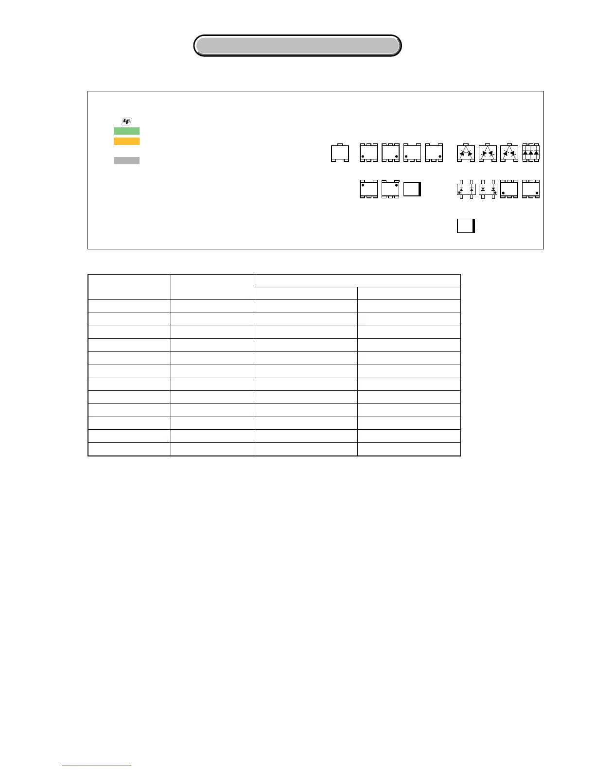
4-3. PRINTED WIRING BOARDS
4-3. PRINTED WIRING BOARDS
• : Uses unleaded solder.
•
: Circuit board
: Flexible board
Pattern from the side which enables seeing.
: pattern of the rear side
(The other layers’ patterns are not indicated)
• Through hole is omitted.
• Circled numbers refer to waveforms.
• There are a few cases that the part printed on diagram
isn’t mounted in this model.
• C: panel designation
THIS NOTE IS COMMON FOR PRINTED WIRING BOARDS
21
3
21
3
21
3
345
21
123
654
EB
C
31
5
2
46
123
654
31
5
2
46
123
54
43
12
312
45
534
12
14
23
46
2
5
31
12
4
3
14
23
• Chip parts.
Transistor Diode
4-3. PRINTED WIRING BOARDS
Board Name Parts Location
Pattern
Total Number of Layers Layers Not Indicated
CD-515 flexible 4-71 2 layers –
ST-111 4-73 4 layers 2 to 3 layers
FL-147 – 4 layers 2 to 3 layers
PL-001 flexible – 1 layers –
CF-099 4-71 4 layers 2 to 3 layers
BB-005 flexible – 2 layers –
MS-211 flexible – 2 layers –
JK-269 flexible – 1 layer –
AF-008 flexible – 1 layer –
BT-026 flexible – 1 layer –
RE-003 flexible – 1 layer –
LI-072 flexible – 1 layer –