56
DVP-S9
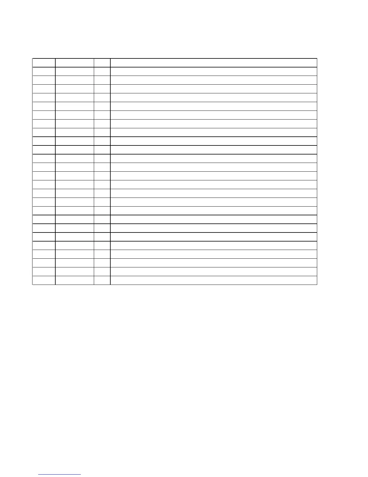
Pin No. Pin Name I/O Description
62 VCC —
Power supply terminal (+5V)
63
SOFT-TEST
O
For software check terminal Not used (open)
64 VSS —
Ground terminal
65 to 68
LED_DISC1 O LED drive signal output of the
1
indicator (D705) “L”: LED on
69 to 72
LED_DISC2 O LED drive signal output of the
2
indicator (D704) “L”: LED on
73 to 76
LED_DISC3 O LED drive signal output of the
3
indicator (D703) “L”: LED on
77 to 80
LED_PLAY O LED drive signal output of the
N
indicator (D702) “L”: LED on
81 to 83
LED_PAUSE O LED drive signal output of the
X
indicator (D701) “L”: LED on
84
EXP-IN DATA I Serial data input terminal
85
EXP-OUT DATA
O Serial data output terminal
86
EXP-LAT O Serial data latch pulse signal output terminal
87
EXP-CLK O Serial clock signal output terminal
88
LED_PAUSE O LED drive signal output of the
X
indicator (D701) “L”: LED on
89 A-SHUT I
Shut off (deck-A) detection signal input terminal
90 B-SHUT I
Shut off (deck-B) detection signal input terminal
91
B-HALF
I
Detection input terminal from the deck-B cassette detect switch “L”: cassette in
92
MODEL-IN I Model destination setting terminal
93
PWRCHK — Power check terminal Fixed at “H”
94
KEY2 I Key input terminal
95
KEY1 I Key (S711 to S720) input terminal (A/D input)
96 AVSS —
Ground terminal (for A/D converter)
97
KEY0 I Key (S701 to S708) input terminal (A/D input)
98
VREF
I
Reference voltage (+5V) input terminal (for A/D converter)
99 AVCC —
Power supply terminal (+5V) (for A/D converter)
100
NC — Not used (open)


 To Next Page