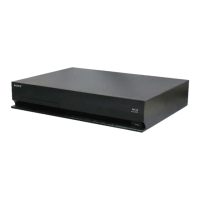
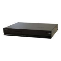
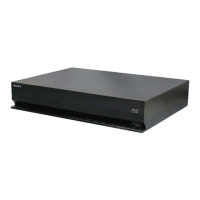
HBD-E370/E470/E570/E870/T57
82
Pin No. Pin Name I/O Description
AC3 FE_LVDS_3P - Not used
AC5 FE_LVDS_5P - Not used
AC7 FE_AVDD12_4 - Power supply terminal (+1.2V)
AC9 FE_DVDD33O - Power supply terminal (+3.3V)
AC21 DVSS - Ground terminal
AC23 DVSS - Ground terminal
AC25 DVSS - Ground terminal
AC27 DVSS - Ground terminal
AC29 DVSS - Ground terminal
AC31 DVSS - Ground terminal
AC37 B_RA5 O Address signal output to the SD-RAM
AC39 B_RBA2 O Bank address signal output to the SD-RAM
AC41 B_RCKE O Clock enable signal output to the SD-RAM
AC43 B_RWEB O Write enable signal output to the SD-RAM
AD2 FE_CFREQ I/O Serial data input/output with the BD drive
AD4 FE_FOO O Motor drive signal output to the motor driver IC
AD6 FE_GAINSW2 O Read/write gain switch dignal output to the motor driver IC
AD8 FE_GIO0 O Motor drive muting on/off control signal output to the motor driver IC
AD20 VCCK - Power supply terminal (+1.1V)
AD22 VCCK - Power supply terminal (+1.1V)
AD24 DVSS - Ground terminal
AD26 DVSS - Ground terminal
AD28 DVSS - Ground terminal
AD30 VCCK - Power supply terminal (+1.1V)
AD32 VCCK - Power supply terminal (+1.1V)
AD36 B_RBA1 O Bank address signal output to the SD-RAM
AD38 B_RA9 O Address signal output to the SD-RAM
AD40 B_RBA0 O Bank address signal output to the SD-RAM
AD42 B_RCSB O Chip select signal output to the SD-RAM
AE1 FE_FMO O Motor drive signal output to the motor driver IC
AE3 FE_TRAYPWM O Motor drive signal output to the motor driver IC
AE5 FE_GAINSW1 O Read/write gain switch dignal output to the motor driver IC
AE7 FE_OSOEN O Serial data transfer clock signal output to the BD drive
AE9 FE_GIO12 - Not used
AE21 DVSS - Ground terminal
AE23 DVSS - Ground terminal
AE25 DVSS - Ground terminal
AE27 DVSS - Ground terminal
AE29 DVSS - Ground terminal
AE31 DVSS - Ground terminal
AE35 DVSS - Ground terminal
AE37 DVSS - Ground terminal
AE39 DVSS - Ground terminal
AE41 B_RA12 O Address signal output to the SD-RAM
AE43 B_RA7 O Address signal output to the SD-RAM
AF2 FE_DMO O Motor drive signal output to the motor driver IC
AF4 FE_FMO2 O Motor drive signal output to the motor driver IC
AF6 FE_FMO4 O Motor drive signal output to the motor driver IC
AF8 FE_CMOD O Serial interface commande enable signal output to the BD drive
AF20 VCCK - Power supply terminal (+1.1V)
AF22 VCCK - Power supply terminal (+1.1V)
AF24 DVSS - Ground terminal
AF26 DVSS - Ground terminal
AF28 DVSS - Ground terminal
AF30 VCCK - Power supply terminal (+1.1V)
AF32 VCCK - Power supply terminal (+1.1V)
AF36 B_RA10 O Address signal output to the SD-RAM
AF38 B_RA1 O Address signal output to the SD-RAM
AF40 VCC2IO - Power supply terminal (+1.8V)
AF42 VCC2IO - Power supply terminal (+1.8V)
w
w
w
.
x
i
a
o
y
u
1
6
3
.
c
o
m
Q
Q
3
7
6
3
1
5
1
5
0
9
9
2
8
9
4
2
9
8
T
E
L
1
3
9
4
2
2
9
6
5
1
3
9
9
2
8
9
4
2
9
8
0
5
1
5
1
3
6
7
3
Q
Q
TEL 13942296513 QQ 376315150 892498299
TEL 13942296513 QQ 376315150 892498299
http://www.xiaoyu163.com
http://www.xiaoyu163.com