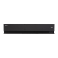
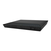
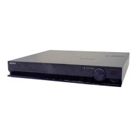
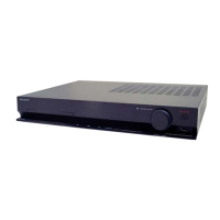
HBD-E370/E470/E570/E870/T57
83
Pin No. Pin Name I/O Description
AG1 FE_GIO3 - Not used
AG3 FE_LIMIT I Sledge innner limit signal input from the motor driver IC
AG5 FE_GAINSW3 - Not used
AG7 FE_FMO3 O Motor drive signal output to the motor driver IC
AG9 FE_GIO1 O Motor drive muting on/off control signal output to the motor driver IC
AG21 DVSS - Ground terminal
AG23 DVSS - Ground terminal
AG25 DVSS - Ground terminal
AG27 DVSS - Ground terminal
AG29 DVSS - Ground terminal
AG31 DVSS - Ground terminal
AG37 B_RA2 O Address signal output to the SD-RAM
AG39 B_RA6 O Address signal output to the SD-RAM
AG41 B_RODT O On die termination enable signal output to the SD-RAM
AG43 B_RA0 O Address signal output to the SD-RAM
AH2 FE_PLAY# - Not used
AH4 FE_EJECT# I Eject/stop key input from the system controller
AH6 FE_TRO O Motor drive signal output to the motor driver IC
AH8 FE_FSOURCE - Not used
AH20 VCCK - Power supply terminal (+1.1V)
AH22 VCCK - Power supply terminal (+1.1V)
AH24 DVSS - Ground terminal
AH26 DVSS - Ground terminal
AH28 DVSS - Ground terminal
AH30 VCCK - Power supply terminal (+1.1V)
AH32 VCCK - Power supply terminal (+1.1V)
AH36 B_RA8 O Address signal output to the SD-RAM
AH38 B_RA11 O Address signal output to the SD-RAM
AH40 B_RCASB O Column address strobe signal output to the SD-RAM
AH42 B_RA4 O Address signal output to the SD-RAM
AJ1 FE_XTAL25MO - Not used
AJ3 FE_XTAL25MI I System clock signal input terminal (25 MHz)
AJ5 FE_TRAYIN# I Disc tray in detection signal input terminal
AJ7 DVSS_XTAL - Ground terminal
AJ9 VCLK25MI O System clock signal output terminal (25 MHz)
AJ21 DVSS - Ground terminal
AJ23 VCCK - Power supply terminal (+1.1V)
AJ25 VCCK - Power supply terminal (+1.1V)
AJ27 VCCK - Power supply terminal (+1.1V)
AJ29 VCCK - Power supply terminal (+1.1V)
AJ31 DVSS - Ground terminal
AJ35 DVSS - Ground terminal
AJ37 DVSS - Ground terminal
AJ39 DVSS - Ground terminal
AJ41 B_RRASB O Row address strobe signal output to the SD-RAM
AJ43 B_RA3 O Address signal output to the SD-RAM
AK2 USB_DM0 I/O USB differential serial data (negative) input/output with the USB connector (rear side)
AK4 FE_TRAYOUT I Disc tray out detection signal input terminal
AK6 AVSS12_USB - Ground terminal
AK8 AVDD12_USB - Power supply terminal (+1.2V)
AK20 VCCK - Power supply terminal (+1.1V)
AK22 DVSS - Ground terminal
AK24 DVSS - Ground terminal
AK26 DVSS - Ground terminal
AK28 DVSS - Ground terminal
AK30 DVSS - Ground terminal
AK32 VCCK - Power supply terminal (+1.1V)
AK36 B_RDQ9 I/O Two-way data bus with the SD-RAM
AK38 B_RA13 O Address signal output to the SD-RAM
AK40 VCC2IO - Power supply terminal (+1.8V)
w
w
w
.
x
i
a
o
y
u
1
6
3
.
c
o
m
Q
Q
3
7
6
3
1
5
1
5
0
9
9
2
8
9
4
2
9
8
T
E
L
1
3
9
4
2
2
9
6
5
1
3
9
9
2
8
9
4
2
9
8
0
5
1
5
1
3
6
7
3
Q
Q
TEL 13942296513 QQ 376315150 892498299
TEL 13942296513 QQ 376315150 892498299
http://www.xiaoyu163.com
http://www.xiaoyu163.com