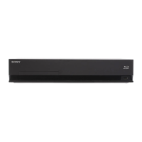
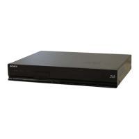
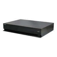
HBD-E770W
86
Pin No. Pin Name I/O Description
AR41 B_RDQS1B O Data strobe signal (negative) output to the SD-RAM
AR43 B_RDQS1 O Data strobe signal (positive) output to the SD-RAM
AT2 XI_RTC I Not used
AT4 XO_RTC O Not used
AT6 AVSS12_ADC - Ground terminal
AT10 FE_GIO13 - Not used
AT12 SCL I/O Two-way clock bus with the EEPROM
AT14 DVSS - Ground terminal
AT16 A_RDQ5 I/O Two-way data bus with the SD-RAM
AT18 A_RDQM0 O Data mask signal output to the SD-RAM
AT20 A_RDQ11 I/O Two-way data bus with the SD-RAM
AT22 DVSS - Ground terminal
AT24 A_RA11 O Address signal output to the SD-RAM
AT26 A_RA1 O Address signal output to the SD-RAM
AT28 A_RBA2 O Bank address signal output to the SD-RAM
AT30 A_RVREF I Reference voltage (+0.9V) input terminal for the SD-RAM
AT32 A_RDQ23 I/O Two-way data bus with the SD-RAM
AT34 DVSS - Ground terminal
AT36 DVSS - Ground terminal
AT38 B_RDQ5 I/O Two-way data bus with the SD-RAM
AT40 B_RDQS0 O Data strobe signal (positive) output to the SD-RAM
AT42 B_RDQS0B O Data strobe signal (negative) output to the SD-RAM
AU1 AVDD33_RTC - Power supply terminal (+3.3V)
AU3 AVSS33_RTC - Ground terminal
AU5 AVDD33_SACD - Power supply terminal (+3.3V)
AU7 AVDD33_ST - Power supply terminal (+3.3V)
AU9 AVSS12_ST2 - Ground terminal
AU11 EEPWRQ - Not used
AU13 VCC3IO_1 - Power supply terminal (+3.3V)
AU15 A_RDQ3 I/O Two-way data bus with the SD-RAM
AU17 DVSS - Ground terminal
AU19 A_RDQ9 I/O Two-way data bus with the SD-RAM
AU21 DVSS - Ground terminal
AU23 A_RCASB O Column address strobe signal output to the SD-RAM
AU25 DVSS - Ground terminal
AU27 A_RBA1 O Bank address signal output to the SD-RAM
AU29 DVSS - Ground terminal
AU31 A_RDQ21 I/O Two-way data bus with the SD-RAM
AU33 DVSS - Ground terminal
AU35 A_RDQM3 O Data mask signal output to the SD-RAM
AU37 A_RDQ27 I/O Two-way data bus with the SD-RAM
AU39 DVSS - Ground terminal
AU41 B_RDQ3 I/O Two-way data bus with the SD-RAM
AU43 B_RDQ2 I/O Two-way data bus with the SD-RAM
AV2 FE_JRTCLK - Not used
AV4 AVSS33_SACD - Ground terminal
AV6 AVDD12_SRX1 - Power supply terminal (+1.2V)
AV8 AVSS12_ST1 - Ground terminal
AV10 AVDD12_ST - Power supply terminal (+1.2V)
AV12 GPIO6 O UPG status signal output to the system controller
AV14 SDA I/O Two-way data bus with the EEPROM
AV16 A_RDQ0 I/O Two-way data bus with the SD-RAM
AV18 A_RDQM1 O Data mask signal output to the SD-RAM
AV20 A_RDQ14 I/O Two-way data bus with the SD-RAM
AV22 A_RA13 O Address signal output to the SD-RAM
AV24 A_RCSB O Chip select signal output to the SD-RAM
AV26 A_RA2 O Address signal output to the SD-RAM
AV28 A_RA5 O Address signal output to the SD-RAM
AV30 NC - Not used
w
w
w
.
x
i
a
o
y
u
1
6
3
.
c
o
m
Q
Q
3
7
6
3
1
5
1
5
0
9
9
2
8
9
4
2
9
8
T
E
L
1
3
9
4
2
2
9
6
5
1
3
9
9
2
8
9
4
2
9
8
0
5
1
5
1
3
6
7
3
Q
Q
TEL 13942296513 QQ 376315150 892498299
TEL 13942296513 QQ 376315150 892498299
http://www.xiaoyu163.com
http://www.xiaoyu163.com