57
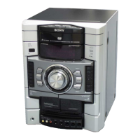
HCD-GNX80
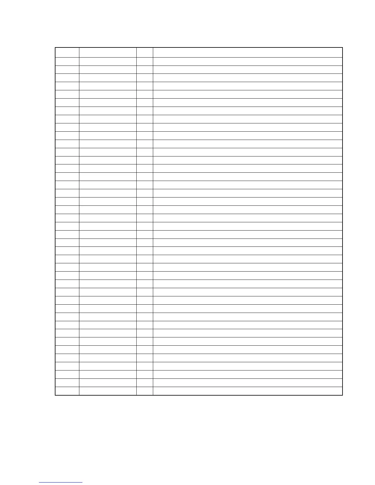
Pin No. Pin Name I/O Description
1 to 8 G8 to G1 O FLD grid signal output
9, 10 P1,P2 O FLD segment signal output
11 VSS-IO — Ground
12 to 22 P3 to P13 O FLD segment signal output
23 VDD-FIP — Power supply (+3.3V)
24 to 41 P14 to P31 O FLD segment signal output
42 VSS-IO — Ground
43 to 47 P32 to P36 O FLD segment signal output
48 VKK — Power supply (-35V)
49 MD0 I MD0 signal at test
50 MD1/VDD-VFT I Not used (pull down)
51 MD2 I Not used (pull down)
52 LED CD/DVD O LED drive signal output
53 LED TUNER O LED drive signal output
54 LED TAPE O LED drive signal output
55 LED VIDEO O LED drive signal output
56 LED STOP,PAUSE O LED drive signal output
57 LED VOLUME 2,3 O LED drive signal output
58 LED VOLUME 3,4 O LED drive signal output
59 LED VOLUME 6,1 O LED drive signal output
60 IIC DATA I/O IIC bus serial data input/output
61 IIC CLK I/O IIC bus serial clock input/output
62 AVCC — Power supply (+3.3V)
63 AVSS — Ground
64 to 66 KEY0 to KEY2 I Key input (A/D)
67 ALL BAND I Audio L+R signal input
68 to 71 BPF4 to BPF1 I Spectrum analyzer signal input
72 LED AUX/GAME O LED drive signal output
73 JOG X-ROUND O LED drive signal output (not used)
74 VOLUME I Volume encoder signal input
75 JOG I JOG dial encoder signal input
76 AMS I AMS dial signal input
77 RESET I Reset input
78 LED AMS+/-,FF/FW O LED drive signal output
79 LED PLAY O LED drive signal output
80 SELECTOR O LED group select signal output
81 VSS-CPU — Ground
82 XOUT O Crystal oscillator output (4MHz)
83 XIN I Crystal oscillator input (4MHz)
84 VCC-CPU — Power supply (+3.3V)
85 to 100 G24 to G9 O FLD grid signal output
• IC902 MB90M407PF-G-144-BNDE1 DISPLAY CONTROL (PANEL Board)


 To Next Page