57
HCD-RV22/RV55
• IC371 BU2099FV (SP DRIVER) (MAIN BOARD (2/2))
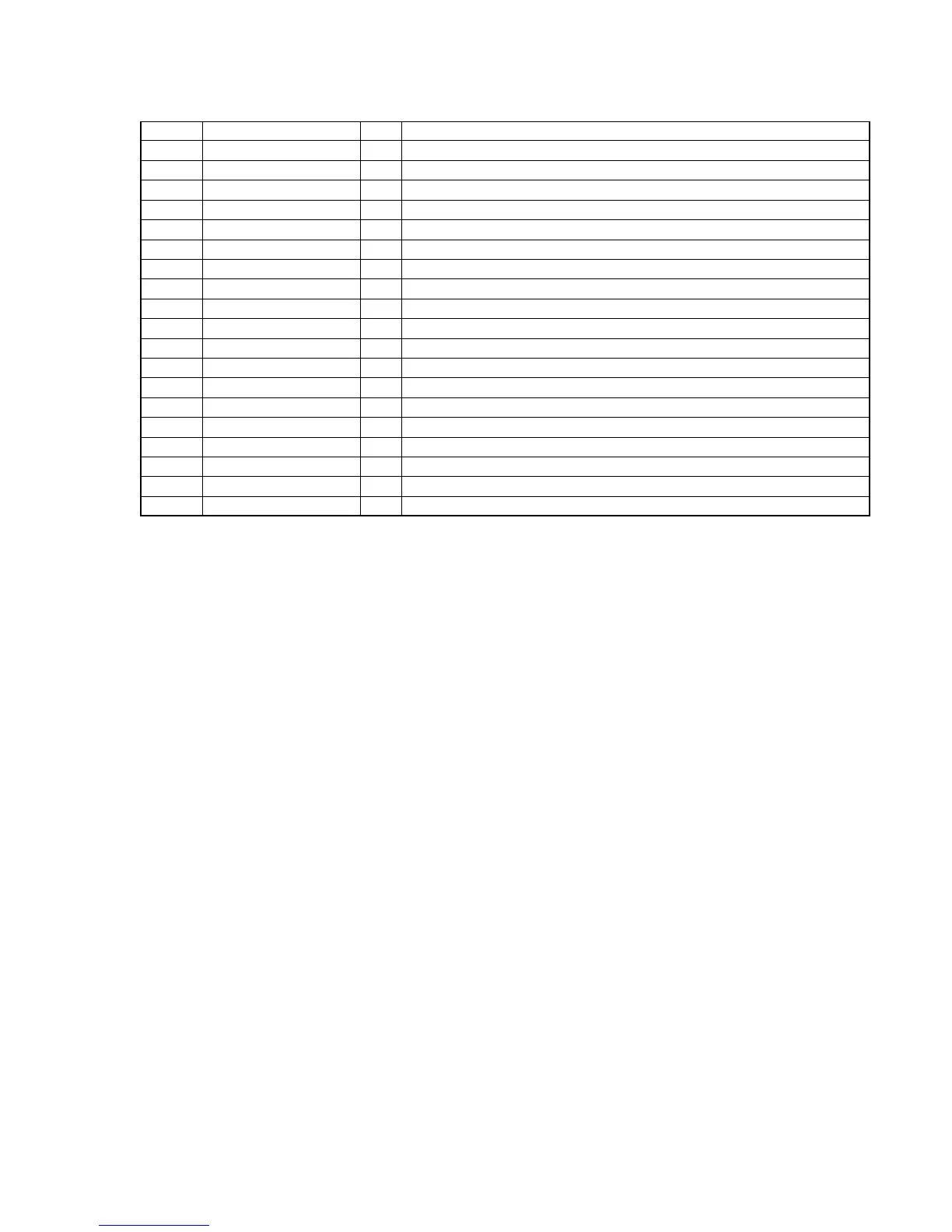
Pin No. Pin Name I/O Pin Description
1 VSS — Ground pin
2 N.C. — Not used. (Open)
3DATAISerial data input from the motor/plunger driver
4 CLOCK I Serial data transfer clock signal input from the system controller
5 LCH I Latch pulse signal input from the system controller
6Q0ORecording/playback selection signal output
7Q1ORecording bias control signal output
8, 9 Q2, Q3 O Not used. (Fixed at “L” in this set.)
10 Q4 O CD muting on/off control signal output
11 Q5 O Tuner muting on/off control signal output
12 Q6 O Power amplifier on/off control signal output
13 Q7 O Loading motor drive signal output
14 Q8 O Loading motor drive signal output
15 Q9 O Table motor drive signal output
16 Q10 O Table motor drive signal output
17 Q11 O Front speaker on/off relay drive control signal output
18 SO O Serial data output Not used (Connect to ground in this set.)
19 OE — Not used. (Open)
20 VDD — Power supply pin (+3.3 V)


 To Next Page