52
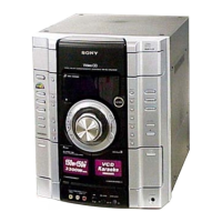
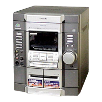
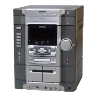
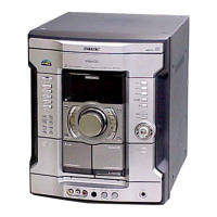
HCD-RV22/RV55
• IC Pin Function Description
• IC505 CXD1887R (DIGITAL SIGNAL PROCESSOR, DIGITAL SERVO PROCESSOR,
MPEG VIDEO/AUDIO DECODER, VIDEO SIGNAL ENCODER) (VMP43GY BOARD (2/2))
Pin No. Pin Name I/O Pin Description
1VBOConnected to ground via a capacitor.
2 IREF O D/A converter reference current output
3 VRF I D/A converter reference voltage input
4VGOConnected to the analog power supply (+2.5 V) via a capacitor.
5 XCPSIG O Luminance video composite/component signal invert output Not used. (Fixed at “L”.)
6 CPSIG O Luminance video composite/component signal output
7, 8 NC — Not used. (Pin 7: Open, Pin 8: Fixed at “H”.)
9V AVS2 — Analog ground pin (for D/A converter)
10 IVD1 — Power supply pin (+3.3 V) (for I/O)
11 I2C CLK I/O
Communication data reading clock signal input or transfer clock signal output
Not used. (Open)
12 I2C DATA I/O Communication data bus pin Not used. (Open)
13 GPIO0 I Serial data input from the system controller
14 GPIO1 O Serial data output to the system controller
15 GPIO2 O Serial data transfer clock signal output to the system controller
16 GIPO3 I Request signal input from the system controller
17 LVD1 — Digital power supply pin (+2.5 V) (for AV decoder block)
18 GPIO4 I Acknowledge signal input from the system controller
19 GPIO5 O Chip select signal output to the system controller
20, 21 GPIO6, GPIO7 I/O Not used. (Open)
22 LVS1 — Digital ground pin (for AV decoder block)
23 GPIO8 I/O Not used. (Open)
24 GPIO9 O Frequency selection signal output
25 GPIO10 I/O Not used. (Open)
26 GPIO11 O Serial data latch pulse signal output to the digital filter
27 LVD2 — Digital power supply pin (+2.5 V) (for AV decoder block)
28 GPIO12 O Control signal output to the D/A converter
29 GPIO13 O Serial data transfer clock signal output to the digital filter and D/A conveter
30 GPIO14 O Serial data output to the digital filter and D/A converter
31 IVS1 — Ground pin (for I/O)
32 LVS2 — Digital ground pin (for AV decoder block)
33 IVD2 — Power supply pin (+3.3 V) (for I/O)
34 to 37 DRADR0 to DRADR3 O Address signal output to the D-RAM and program ROM
38 LVD3 — Digital power supply pin (+2.5 V) (for AV decoder block)
39 to 45 DRADR4 to DRADR10 O Address signal output to the D-RAM and program ROM
46 LVS3 — Digital ground pin (for AV decoder block)
47 IVS2 — Ground pin (for I/O)
48 IVD3 — Power supply pin (+3.3 V) (for I/O)
49 to 56 DRDAT0 to DRDAT7 I/O Two-way data bus with the D-RAM Data input from the program ROM
57 IVS3 — Ground pin (for I/O)
58 IVD4 — Power supply pin (+3.3 V) (for I/O)
59 to 66 DRDAT8 to DRDAT15 I/O Two-way data bus with the D-RAM Data output to the program ROM
w
w
w
.
x
i
a
o
y
u
1
6
3
.
c
o
m
Q
Q
3
7
6
3
1
5
1
5
0
9
9
2
8
9
4
2
9
8
T
E
L
1
3
9
4
2
2
9
6
5
1
3
9
9
2
8
9
4
2
9
8
0
5
1
5
1
3
6
7
3
Q
Q
TEL 13942296513 QQ 376315150 892498299
TEL 13942296513 QQ 376315150 892498299
http://www.xiaoyu163.com
http://www.xiaoyu163.com