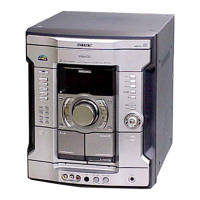
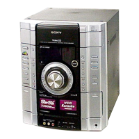
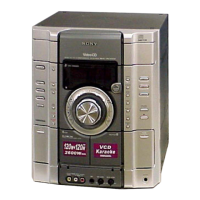
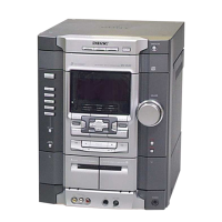
53
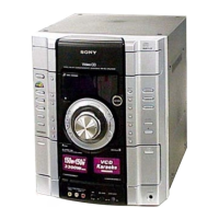
HCD-RV22/RV55
Pin No. Pin Name I/O Pin Description
67 IVS4 — Ground pin (for I/O)
68 DRCAS O Column address strobe signal output to the D-RAM
69 LVD4 — Digital power supply pin (+2.5 V) (for AV decoder block)
70 DRCK O Clock signal output to the D-RAM
71 IVD5 — Power supply pin (+3.3 V) (for I/O)
72 DRRAS O Row address strobe signal output to the D-RAM
73 DRWEL O Write enable signal output to the D-RAM
74 NVOEL O Chip select signal output to the D-RAM
75 LVS4 — Digital ground pin (for AV decoder block)
76 DRBS O Bank select signal output to the D-RAM
77, 78 DRDQM0, DRDQM1 O Mask control signal output to the D-RAM
79 IVS5 — Ground pin (for I/O)
80 NC — Not used. (Open)
81 SYSRST I Reset signal input from the system controller “L”: reset
82 IRDIN I IR data input pin Not used. (Open)
83 NC — Not used. (Open)
84 VDD1 — Digital power supply pin (+2.5 V) (for CD-DSP block)
85 V16M O Wide-band EFM PLL VCO2 oscillation output Not used. (Open)
86 DOUT O Digital audio signal output Not used. (Open)
87 L CDLRCK I L/R sampling clock signal (44.1 kHz) input
88 LRCK O L/R sampling clock signal (44.1 kHz) output
89 VSS1 — Digital ground pin
90 L CDDATA I Serial data input
91 PCMD O Serial data output
92 L CDBCK I Bit clock signal (2.8224 MHz) input
93 BCK O Bit clock signal (2.8224 MHz) output
94 EMPH O
“L” is output when playback disc is emphasis off
“H” is output when playback disc is emphasis on Not used. (Open)
95 L SQSO I Subcode-Q 80-bit, PCM peak and level data, CD text data input
96 SQSO O Subcode-Q 80-bit, PCM peak and level data, CD text data output
97 VDD2 — Digital power supply pin (+2.5 V) (for CD-DSP block)
98 L SQCK O SQSO readout clock signal output
99 SQCK I SQSO readout clock signal input
100 SBSO O Subcode P to W serial data ooutput Not used. (Open)
101 EXCK I SBSO readout clock signal input Not used. (Fixed at “L”.)
102 DATA I Serial data input
103 L DDAT O Serial data output
104 VSS2 — Digital ground pin
105 L CDXRST O Reset signal output “L”: reset
106 XRST I Reset signal input “L”: reset
107 MUTE I Muting on/off control signal input. “H”: muting on Not used. (Fixed at “L”.)
108 L XLAT O Serial data latch pulse signal output
109 XLAT I Serial data latch pulse signal input
110 L DCLK O Serial data transfer clock signal output
111 CLOK I Serial data transfer clock signal input
w
w
w
.
x
i
a
o
y
u
1
6
3
.
c
o
m
Q
Q
3
7
6
3
1
5
1
5
0
9
9
2
8
9
4
2
9
8
T
E
L
1
3
9
4
2
2
9
6
5
1
3
9
9
2
8
9
4
2
9
8
0
5
1
5
1
3
6
7
3
Q
Q
TEL 13942296513 QQ 376315150 892498299
TEL 13942296513 QQ 376315150 892498299
http://www.xiaoyu163.com
http://www.xiaoyu163.com