21
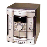
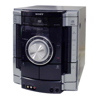
HCD-RV660D/RV990D
6. IC PIN DESCRIPTIONS
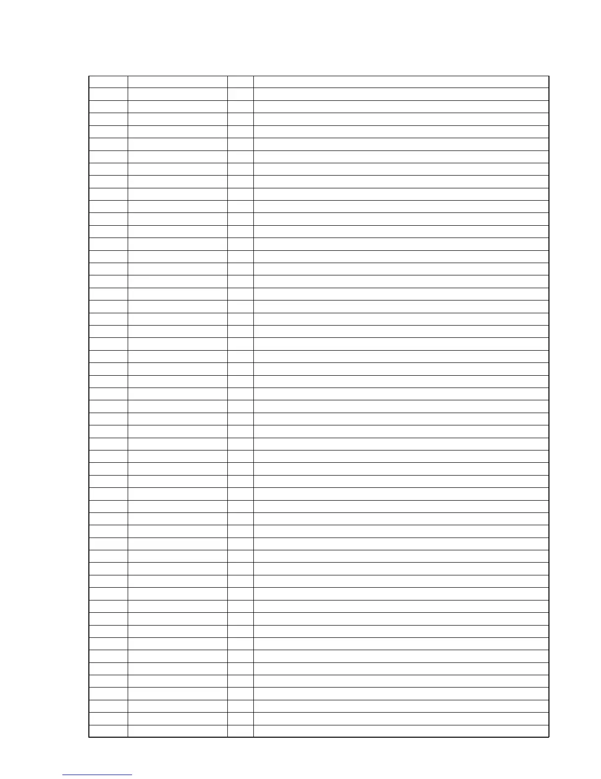
• IC701 TMC57929PGF-RDP (DVD DECODER) (DMB03 Board (3/8))
Pin No. Pin Name I/O Pin Description
1, 2 D5, D6 I/O Two-way data bus signal input from/output to mechanism control IC.
3 VSS — Ground
4D7I/O Two-way data bus signal input from/output to mechanism control IC.
5A0I/O Address signal input from/output to mechanism control IC.
6 VDD — Power supply pin (+3.2 V)
7A1I/O Address signal input from/output to mechanism control IC.
8 VDD5V — Power supply pin (+5 V)
9 to 14 A2 to A7 I/O Address signal input from/output to mechanism control IC.
15 VSS — Ground
16 XWAIT O Not used (Open)
17 XRD I Read strobe signal input from mechanism control IC.
18 XWR I Write strobe signal input from mechanism control IC.
19 XCS I Chip select signal input from mechanism control IC.
20, 21 XINT0, XINT1 O Interrupt signal output to mechanism control IC.
22 VDD — Power supply pin (+3.2 V)
23 XHRS I Not used (Open)
24 HDB7 I/O Stream data input from/output to DVD system processor IC.
25 VSS — Ground
26 HDB8 I/O Error flag signal input from/output to DVD system processor IC.
27 HDB6 I/O Stream data input from/output to DVD system processor IC.
28 VDDS — Power supply pin (+5 V)
29 HDB9 I/O Not used (Open)
30 HDB5 I/O Stream data input from/output to DVD system processor IC.
31 HDBA I/O Not used (Open)
32 HDB4 I/O Stream data input from/output to DVD system processor IC.
33 VSS — Ground
34 HDBB I/O Not used (Open)
35 HDB3 I/O Stream data input from/output to DVD system processor IC.
36 VDD — Power supply pin (+3.2 V)
37 HDBC I/O Not used (Open)
38 VDDS — Power supply pin (+5 V)
39 HDB2 I/O Stream data input from/output to DVD system processor IC.
40 HDBD I/O Not used (Open)
41 HDB1 I/O Stream data input from/output to DVD system processor IC.
42 VSS — Ground
43 HDBE I/O Not used (Open)
44 HDBO I/O Stream data input from/output to DVD system processor IC.
45 HDBF I/O Not used (Open)
46 HDRQ O Serial data effect flag signal output to DVD system processor IC.
47 VDDS — Power supply pin (+5 V)
48 XHWR I Serial data transfer clock signal input from DVD system processor IC.
49 XHRD I Not used (Open)
50 VDD — Power supply pin (+3.2 V)
51 REDY O Not used (Open)
52 VSS — Ground
53 XHAC I Serial data request signal input from DVD system processor IC. (DVD mode)
54 HINT I/O Not used (Fixed at H)
55 XS16 I Not used (Fixed at H)
56 HA1 I Not used (Fixed at H)
57 XPDI I/O Not used (Fixed at H)
58 VDDS — Power supply pin (+5 V)
59, 60 HA0, HA2 I Not used (Fixed at H)
 Loading...