– 89 –
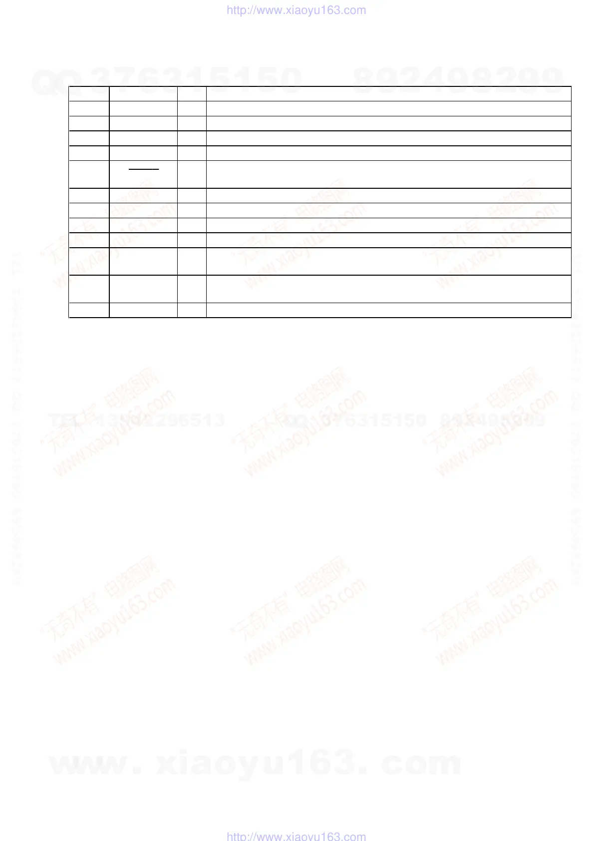
Pin No. Pin Name I/O Description
69 VDD —
Power supply terminal (+5V)
70 XIN I
System clock input terminal (12.5 MHz)
71 VSS —
Ground terminal
72 XOUT O
System clock output terminal (12.5 MHz)
73 RESET I
System reset signal input from the reset signal generator (IC502) “L”: reset
For several hundreds msec. after the power supply rises, “L” is input, then it changes to “H”
74 CH O
Not used (open)
75 BUSY I
Not used (fixed at “L”)
76 TEST I
Connected to ground
77 GRAD R1 O
Not used (open)
78 I2C DATA I/O
Communication data bus with the system controller (IC501) and CD mechanism controller
(IC502)
79 I2C CLK I/O
Communication data reading clock signal input or transfer clock signal output with the system
controller (IC501) and CD mechanism controller (IC502)
80 GRAD R2 O
Not used (open)
w
w
w
.
x
i
a
o
y
u
1
6
3
.
c
o
m
Q
Q
3
7
6
3
1
5
1
5
0
9
9
2
8
9
4
2
9
8
T
E
L
1
3
9
4
2
2
9
6
5
1
3
9
9
2
8
9
4
2
9
8
0
5
1
5
1
3
6
7
3
Q
Q
TEL 13942296513 QQ 376315150 892498299
TEL 13942296513 QQ 376315150 892498299
http://www.xiaoyu163.com
http://www.xiaoyu163.com