4-40
HXR-MC1/MC1P
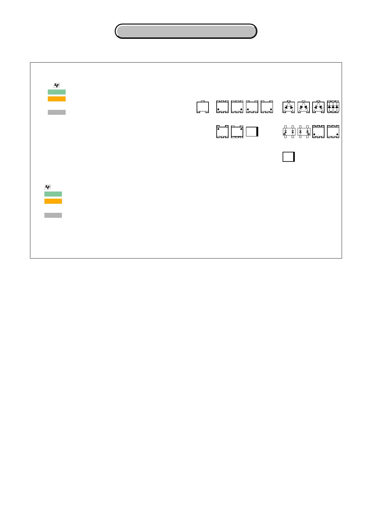
4-3. PRINTED WIRING BOARDS
4-3. PRINTED WIRING BOARDS
4-3. PRINTED WIRING BOARDS
• : Uses unleaded solder.
•
: Circuit board
: Flexible board
Pattern from the side which enables seeing.
: pattern of the rear side
(The other layers’ patterns are not indicated)
• Through hole is omitted.
• There are a few cases that the part printed on diagram
isn’t mounted in this model.
• C: panel designation
(ENGLISH)
THIS NOTE IS COMMON FOR PRINTED WIRING BOARDS
(JAPANESE)
21
3
21
3
21
3
345
21
123
654
EB
C
31
5
2
46
123
654
31
5
2
46
123
54
43
12
312
45
534
12
14
23
46
2
5
31
12
4
3
14
23
• Chip parts.
Transistor Diode
プリント図共通ノート
【プリント図ノート】
・ :無鉛半田を使用しています。
・ :基板
:フレキシブル配線板
見ている面側のパターン。
:裏側のパターン
(他のパターンについては表示されていません)
・スルーホールは省略。
・プリント図には,本機で使用していない部品が記載されている
場合があります。
・Cはパネル表示名称。

 Loading...