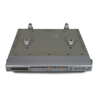
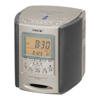
ICF-CDK70
ICF-CDK70
1717
SECTION 6
DIAGRAMS
For Schematic Diagrams.
Note:
• All capacitors are in µF unless otherwise noted. (p: pF)
50 WV or less are not indicated except for electrolytics
and tantalums.
• All resistors are in Ω and
1
/4 W or less unless otherwise
specifi ed.
•
f
: internal component.
• C : panel designation.
THIS NOTE IS COMMON FOR PRINTED WIRING BOARDS AND SCHEMATIC DIAGRAMS.
• A : B+ Line.
• C : adjustment for repair.
• Voltages and waveforms are dc with respect to ground
under no-signal (detuned) conditions.
- CD Board -
no mark : CD play
- TU Board -
no mark : FM
( ) : AM
- Other Boards -
no mark : FM
( ) : CD play
• Voltages are taken with a VOM (Input impedance 10 MΩ).
Voltage variations may be noted due to normal production
tolerances.
• Waveforms are taken with a oscilloscope.
Voltage variations may be noted due to normal production
tolerances.
• Circled numbers refer to waveforms
• Signal path.
F : FM
f : AM
J : CD play
i : AUDIO IN
• Abbreviation
CND : Canadian model
For Printed Wiring Boards.
Note:
• X : parts extracted from the component side.
• Y : parts extracted from the conductor side.
• W : indicated side identifi ed with part number.
•
f
: internal component.
• : Pattern from the side which enables seeing.
(The other layers' patterns are not indicated.)
Note:
The components identi-
fi ed by mark 0 or dotted
line with mark 0 are criti-
cal for safety.
Replace only with part
number specifi ed.
Note:
Les composants identifi és
par une marque 0 sont
critiques pour la sécurité.
Ne les remplacer que par
une piéce portant le nu-
méro spécifi é.
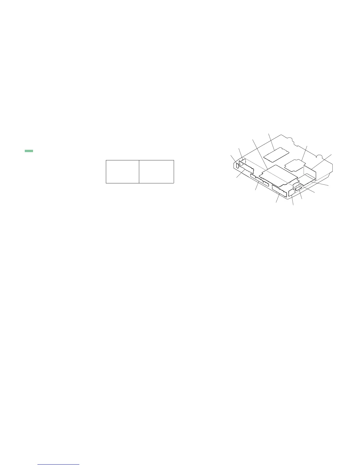
• Circuit Boards Location
MEGA BASS board
JACK board
LCD board
TIMER board
VOL board
KEY board
LED board
TU board
MAIN board
POWER board
AMP board
CD board
REMOTE CONTROL board