261Specifications
Appendix
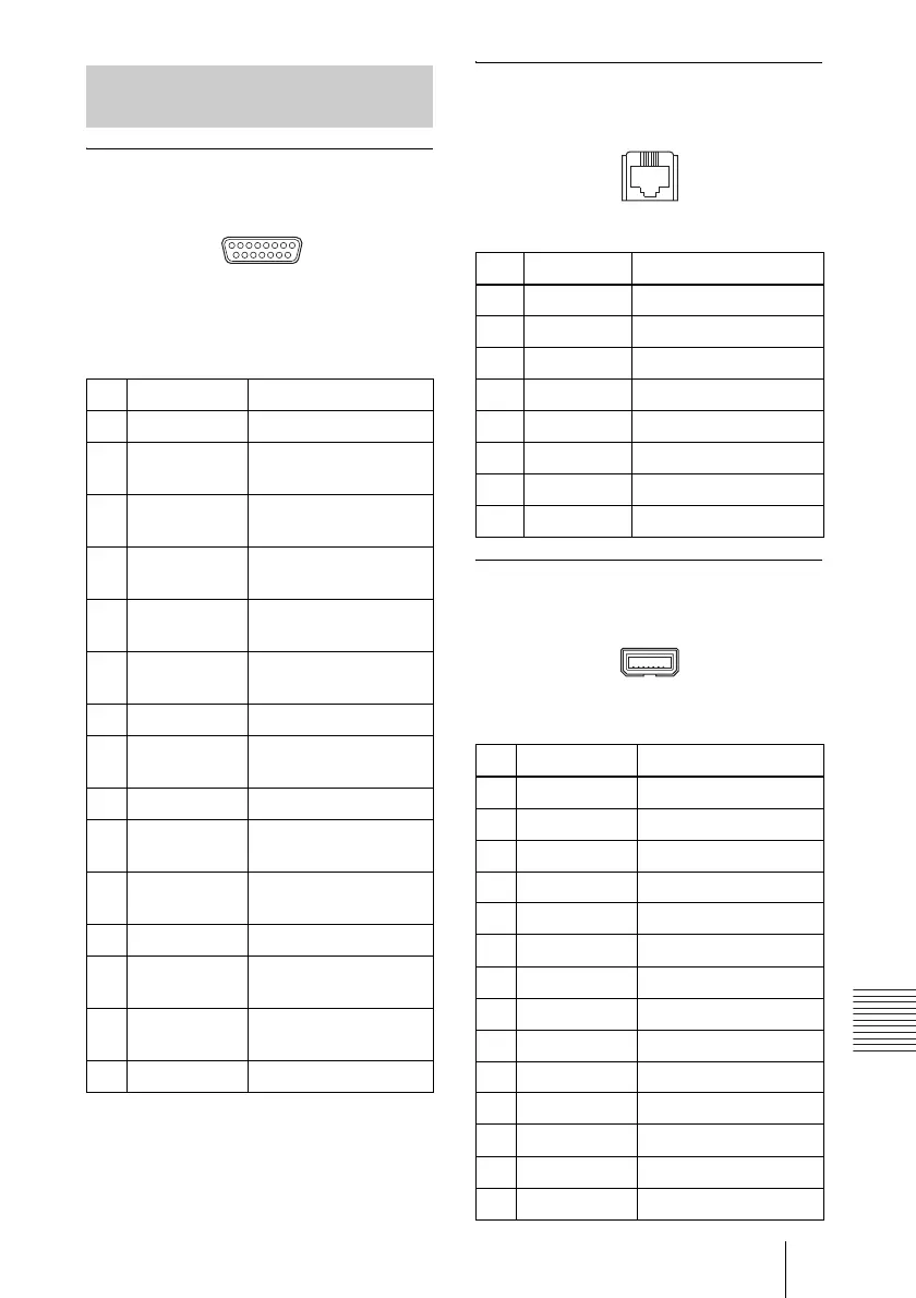
TERMINAL connector
(PCSA-CXG80/CXA55)
D-sub 15-pin connector
(PCSA-CXG80: female/PCSA-CXA55:
male)
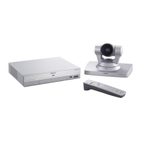
ISDN 1-3 jacks (PCSA-B384S)
ISDN 1-6 jacks (PCSA-B768S)
Modular jack
TERMINAL connector
(PCSA-B384S/PCSA-B768S)
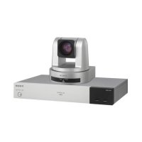
USB connector
Pin Assignments on Optional
Board Connectors
Pin Signal Description
1 Y-OUT Brightness signal
2 Y.GND Brightness signal
ground
3 Pb-OUT Color difference signal
(B – Y)
4 Pb-GND Color difference signal
(B – Y) ground
5 Pr-CAM Color difference signal
(R – Y)
6 Pr-GND Color difference signal
(R – Y) ground
7 No connection –
8No
Connection
–
9 +19.5 V +19.5 V
10 LVDS-TXD+ Multiplexed transmit
signal (+)
11 LVDS-TXD– Multiplexed transmit
signal (-)
12 No connection –
13 LVDX-RXD+ Multiplexed receive
signal (+)
14 LVDS-RXD– Multiplexed receive
signal (-)
15 GND Ground
15 9
81
Pin Signal Description
1NC –
2NC –
3 TA Transmit+
4 RA Receive+
5 RB Receive–
6 TB Transmit–
7NC –
8NC –
Pin Signal Description
1 GND Chassis ground
2 19.5V 19.5V
3 DCLK+ Clock+
4 DCLK– Clock–
5 DR+ Transmit data+
6 DR– Transmit data–
7 FS+ Frame sync+
8 FS– Frame sync–
9 DX+ Receive data+
10 DX– Receive data–
11 TX Serial transmit data
12 RX Serial receive data
13 19.5V 19.5V
14 GND Ground
18
113
214